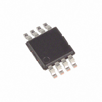
DS1094LU-42M+T Maxim Integrated Products, DS1094LU-42M+T Datasheet - Page 9

DS1094LU-42M+T
Manufacturer Part Number
DS1094LU-42M+T
Description
IC ECONOSCILLATOR SS 8-USOP
Manufacturer
Maxim Integrated Products
Series
EconOscillator™r
Type
Clock Generatorr
Datasheet
1.DS1094LU-42M.pdf
(11 pages)
Specifications of DS1094LU-42M+T
Pll
No
Input
Clock
Output
Clock
Number Of Circuits
1
Ratio - Input:output
2:4
Differential - Input:output
No/No
Frequency - Max
2MHz
Divider/multiplier
Yes/No
Voltage - Supply
3 V ~ 3.6 V
Operating Temperature
-40°C ~ 85°C
Mounting Type
Surface Mount
Package / Case
8-MSOP, Micro8™, 8-uMAX, 8-uSOP,
Frequency-max
2MHz
Lead Free Status / RoHS Status
Lead free / RoHS Compliant
The following terminology is commonly used to
describe 2-wire data transfers.
Master Device: The master device controls the slave
devices on the bus. The master device generates SCL
clock pulses, start, and stop conditions.
Slave Devices: Slave devices send and receive data
at the master’s request.
Bus Idle or Not Busy: Time between stop and start
conditions when both SDA and SCL are inactive and in
their logic high states. When the bus is idle it often initi-
ates a low-power mode for slave devices.
Start Condition: A start condition is generated by the
master to initiate a new data transfer with a slave.
Transitioning SDA from high to low while SCL remains
high generates a start condition. See the timing dia-
gram for applicable timing.
Stop Condition: A stop condition is generated by the
master to end a data transfer with a slave. Transitioning
SDA from low to high while SCL remains high gener-
ates a stop condition. See the timing diagram for
applicable timing.
Repeated Start Condition: The master can use a
repeated start condition at the end of one data transfer
to indicate that it will immediately initiate a new data
transfer following the current one. Repeated starts are
commonly used during read operations to identify a
specific memory address to begin a data transfer. A
repeated start condition is issued identically to a nor-
mal start condition. See the timing diagram for applica-
ble timing.
Figure 3. 2-Wire Timing Diagram
SDA
SCL
Multiphase Spread-Spectrum EconOscillator
STOP
NOTE: TIMING IS REFERENCED TO V
t
BUF
START
2-Wire Serial Interface
t
HD:STA
t
LOW
IL(MAX)
AND V
Description
_____________________________________________________________________
IH(MIN)
t
R
t
HD:DAT
Definitions
.
t
F
t
HIGH
t
SU:DAT
Bit Write: Transitions of SDA must occur during the low
state of SCL. The data on SDA must remain valid and
unchanged during the entire high pulse of SCL plus the
setup and hold time requirements (see Figure 3). Data is
shifted into the device during the rising edge of the SCL.
Bit Read: At the end of a write operation, the master
must release the SDA bus line for the proper amount of
setup time (see Figure 3) before the next rising edge of
SCL during a bit read. The device shifts out each bit of
data on SDA at the falling edge of the previous SCL
pulse, and the data bit is valid at the rising edge of the
current SCL pulse. Remember that the master gener-
ates all SCL clock pulses including when it is reading
bits from the slave.
Acknowledgement
Acknowledgement (ACK) or Not Acknowledge (NACK) is
always the 9th bit transmitted during a byte transfer. The
device receiving data (the master during a read or the
slave during a write operation) performs an ACK by
transmitting a zero during the 9th bit. A device performs
a NACK by transmitting a one during the 9th bit. Timing
(Figure 3) for the ACK and NACK is identical to all other
bit writes. An ACK is the acknowledgement that the
device is properly receiving data. A NACK is used to ter-
minate a read sequence or as an indication that the
device is not receiving data.
Byte Write: A byte write consists of 8 bits of information
transferred from the master to the slave (most significant
bit first) plus a 1-bit acknowledgement from the slave to
the master. The 8 bits transmitted by the master are
done according to the bit write definition, and the
acknowledgement is read using the bit read definition.
Byte Read: A byte read is an 8-bit information transfer
from the slave to the master plus a 1-bit ACK or NACK
from the master to the slave. The 8 bits of information
REPEATED
START
t
SU:STA
t
HD:STA
(ACK
and
t
SP
NACK):
t
SU:STO
An
9


