NB4N507ADG ON Semiconductor, NB4N507ADG Datasheet
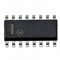
IC SYNTHESIZER CLK PECL 16-SOIC

NB4N507ADG

Manufacturer Part Number
NB4N507ADG
Description
IC SYNTHESIZER CLK PECL 16-SOIC
Manufacturer
ON Semiconductor
Type
Clock/Frequency Synthesizerr
Datasheet

Specifications of NB4N507ADG

Pll
Yes
Input
Clock, Crystal
Output
PECL
Number Of Circuits
1
Ratio - Input:output
1:1
Differential - Input:output
No/Yes
Frequency - Max
200MHz
Divider/multiplier
Yes/Yes
Voltage - Supply
3 V ~ 5.5 V
Operating Temperature
-40°C ~ 85°C
Mounting Type
Surface Mount
Package / Case
16-SOIC (3.9mm Width)
Frequency-max
200MHz
Maximum Input Frequency
52 MHz
Minimum Input Frequency
5 MHz
Output Frequency Range
50 MHz to 200 MHz
Supply Voltage (max)
5.5 V
Supply Voltage (min)
3 V
Maximum Operating Temperature
+ 85 C
Minimum Operating Temperature
- 40 C
Mounting Style
SMD/SMT
Operating Supply Voltage
3.3 V, 5 V
Lead Free Status / RoHS Status
Lead free / RoHS Compliant

Available stocks

Company
Part Number
Manufacturer
Quantity
Price
Part Number:
NB4N507ADG
Manufacturer:
ON Semiconductor
Quantity:
1
Part Number:
NB4N507ADG
Manufacturer:
ON/安森美
Quantity:
20 000
NB4N507A
3.3V/5V, 50 MHz to 200 MHz
PECL Clock Synthesizer
Description
very low jitter differential PECL output clock. It produces a clock
output based on an integer multiple of an input reference frequency.
using Phase-Locked-Loop (PLL) techniques, will produce output
clocks up to 200 MHz. In addition, the PLL circuitry will produce a
50% duty cycle square-wave clock output (see Figure 7).
reference frequency multiples. An exact 155.52 MHz output clock can
be generated from a 19.44 MHz crystal and the x8 multiplier selection.
The NB4N507A is intended for low output jitter clock generation.
and AC terminated. See Figures 4 and 6.
Features
*For additional information on our Pb-Free strategy and soldering details, please
© Semiconductor Components Industries, LLC, 2007
September, 2007 - Rev. 3
download the ON Semiconductor Soldering and Mounting Techniques
Reference Manual, SOLDERRM/D.
The NB4N507A is a precision clock synthesizer which generates a
The NB4N507A accepts a standard fundamental mode crystal,
The NB4N507A can be programmed to generate a selection of input
The PECL outputs are 15 mA open collector and must be DC loaded
Input Crystal Frequency of 10 - 27 MHz
Enable Usage of Common Low-Cost Crystal
Differential PECL Output Clock Frequencies up to 200 MHz
Duty Cycle of 48%/52%
Operating Range: V
Ideal for SONET Applications and Oscillator Manufacturers
Available in Die Form
Packaged in 16-Pin Narrow SOIC
Pb-Free Packages are Available*
Osc
Figure 1. Simplified Logic Block Diagram
CC
PD
= 3.0 V to 5.5 V
CP
VCO
S0
Mult
S1
PECL
1
OE
CLKOUT
CLKOUT
See detailed ordering and shipping information in the package
dimensions section on page 6 of this data sheet.
ORDERING INFORMATION
A
WL
Y
WW
G
MARKING DIAGRAM
http://onsemi.com
= Assembly Location
= Wafer Lot
= Year
= Work Week
= Pb-Free Package
NB4N507AG
CASE 751B
D SUFFIX
AWLYWW
SOIC-16
Publication Order Number:
NB4N507A/D

Related parts for NB4N507ADG

NB4N507ADG Summary of contents

Page 1

... Pb-Free Packages are Available* Osc CP PD Figure 1. Simplified Logic Block Diagram *For additional information on our Pb-Free strategy and soldering details, please download the ON Semiconductor Soldering and Mounting Techniques Reference Manual, SOLDERRM/D. © Semiconductor Components Industries, LLC, 2007 September, 2007 - Rev. 3 CLKOUT PECL VCO CLKOUT ...

Page 2

V DD X1/CLK Oscillator Crystal Buffer X2 Feedback GND X1/CLK GND 5 12 GND CLKOUT 8 Figure 3. 16-Pin SOIC (Top View) ...

Page 3

Table 3. PIN DESCRIPTION Pin # SOIC-16 Name I/O 1 X1/CLK Crystal Input 2,3 V Power Supply Tri-Level Input 5,6 GND Power Supply 7,10,11,12 Connect 15 8 CLKOUT PECL Output* 9 CLKOUT PECL Output* 13 ...

Page 4

Table 6. DC CHARACTERISTICS ( V Symbol I Power Supply Current DD (does not include output load resistor current) V Output HIGH Voltage (Notes 5 & Output LOW Voltage (Notes 5 & Input HIGH ...

Page 5

NB4N507A GND Figure 4. Output Structure V DD NB4N507 PECL Driver GND Figure 5. Evaluation Test Load for the NB4N507A NB4N507A ...

Page 6

... Parallel Crystal Figure 7. Crystal Input Interface ORDERING INFORMATION Device NB4N507AD NB4N507ADG NB4N507ADR2 NB4N507ADR2G †For information on tape and reel specifications, including part orientation and tape sizes, please refer to our Tape and Reel Packaging Specifications Brochure, BRD8011/D. Resource Reference of Application Notes AN1405/D AN1406/D ...

Page 7

NB4N507A Resource Reference of Application Notes AND8001/D - Odd Number Counters Design AND8002/D - Marking and Date Codes AND8020/D - Termination of ECL Logic Devices AND8066/D - Interfacing with ECLinPS AND8090 Characteristics of ECL Devices http://onsemi.com 7 ...

Page 8

... Opportunity/Affirmative Action Employer. This literature is subject to all applicable copyright laws and is not for resale in any manner. PUBLICATION ORDERING INFORMATION LITERATURE FULFILLMENT:  Literature Distribution Center for ON Semiconductor   Box 5163, Denver, Colorado 80217 USA   Phone: 303-675-2175 or 800-344-3860 Toll Free USA/Canada   Fax: 303-675-2176 or 800-344-3867 Toll Free USA/Canada   ...

Related keywords