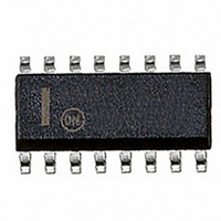
NB4N507ADG ON Semiconductor, NB4N507ADG Datasheet - Page 4

NB4N507ADG
Manufacturer Part Number
NB4N507ADG
Description
IC SYNTHESIZER CLK PECL 16-SOIC
Manufacturer
ON Semiconductor
Type
Clock/Frequency Synthesizerr
Datasheet
1.NB4N507ADR2G.pdf
(8 pages)
Specifications of NB4N507ADG
Pll
Yes
Input
Clock, Crystal
Output
PECL
Number Of Circuits
1
Ratio - Input:output
1:1
Differential - Input:output
No/Yes
Frequency - Max
200MHz
Divider/multiplier
Yes/Yes
Voltage - Supply
3 V ~ 5.5 V
Operating Temperature
-40°C ~ 85°C
Mounting Type
Surface Mount
Package / Case
16-SOIC (3.9mm Width)
Frequency-max
200MHz
Maximum Input Frequency
52 MHz
Minimum Input Frequency
5 MHz
Output Frequency Range
50 MHz to 200 MHz
Supply Voltage (max)
5.5 V
Supply Voltage (min)
3 V
Maximum Operating Temperature
+ 85 C
Minimum Operating Temperature
- 40 C
Mounting Style
SMD/SMT
Operating Supply Voltage
3.3 V, 5 V
Lead Free Status / RoHS Status
Lead free / RoHS Compliant
Available stocks
Company
Part Number
Manufacturer
Quantity
Price
Company:
Part Number:
NB4N507ADG
Manufacturer:
ON Semiconductor
Quantity:
1
Part Number:
NB4N507ADG
Manufacturer:
ON/安森美
Quantity:
20 000
NOTE: Device will meet the specifications after thermal equilibrium has been established when mounted in a test socket or printed circuit
3. PECL output parameters vary 1:1 with V
4. S0 and S1 default to V
NOTE: Device will meet the specifications after thermal equilibrium has been established when mounted in a test socket or printed circuit
5. PECL outputs loaded with external resistors for proper operation (see Figures 4, 5 and 6).
6. V
7. The crystal should be fundamental mode, parallel resonant. Do not use third overtone. For exact tuning when using a crystal, capacitors
8. Guaranteed by design and characterization.
Table 6. DC CHARACTERISTICS (
Table 7. AC CHARACTERISTICS
I
V
V
V
V
C
C
f
f
f
V
DC
PLL
t
t
tr/tf
DD
Xtal
CLK
OUT
jitter (pd)
jitter (pd)
out pk-pk
OH
OL
IH
IL
x
in
Symbol
Symbol
should be connected from pins X1 to ground and X2 to ground. The value of these capacitors is given by the following equation, where CL
is the specified crystal load capacitance: Crystal caps (pF) = (CL-5) x 2. So, for a crystal with 16 pF load capacitance, use two 22 pF caps,
including board trace capacitance (see Figure 7).
OH
BW
board with maintained transverse airflow greater than 500 lfpm. Electrical parameters are guaranteed only over the declared
operating temperature range. Functional operation of the device exceeding these conditions is not implied. Device specification limit
values are applied individually under normal operating conditions and not valid simultaneously.
and V
OL
Power Supply Current
(does not include output load resistor current)
Output HIGH Voltage (Notes 5 & 6)
Output LOW Voltage (Notes 5 & 6)
Input HIGH Voltage (Note 4)
Input LOW Voltage,(Note 4)
Internal Crystal Capacitance, X1 & X2
Input Capacitance, S0, S1, OE
Crystal Input Frequency (Note 7)
Input Clock Frequency (Note 8)
Output Frequency Range
Output Amplitude
Clock Output Duty Cycle (Note 8)
PLL Bandwidth (Note 8)
Period Jitter (RMS, 1s, 10,000 Cycles)
Period Jitter (Peak-to-Peak, 10,000 Cycles)
Output Rise and Fall Times (Note 8)
can be set by the external resistors, which can be modified.
DD
B 2 when left open.
(V
V
Characteristic
Characteristic
DD
DD
DD
= 3.0 V to 5.5 V, GND = 0 V, T
= 3.0 V to 5.5 V, GND = 0 V, T
.
http://onsemi.com
NB4N507A
S0, S1, X1/CLK
S0, S1, X1/CLK
4
V
V
V
DD
DD
DD
V
V
V
DD
DD
DD
= 3.3 V
= 3.3 V
= 3.3 V
A
A
= 5 V
= 5 V
= 5 V
= -40°C to +85°C (Note 5))
= -40°C to +85°C (Note 3))
OE
OE
V
DD
3.95
2.57
3.12
1.90
Min
Min
550
2.0
15
10
10
50
48
10
50
0
5
– 0.5
4.05
2.67
3.20
2.00
Typ
Typ
680
270
5.0
27
23
0
$20
Max
4.15
2.77
3.30
2.10
Max
V
200
500
0.5
0.8
35
30
27
52
52
10
DD
MHz
MHz
MHz
Unit
Unit
kHz
mA
mA
mV
pF
pF
ps
ps
ps
%
V
V
V
V


