LMX2335USLBX National Semiconductor, LMX2335USLBX Datasheet
LMX2335USLBX
Specifications of LMX2335USLBX


Related parts for LMX2335USLBX


LMX2335USLBX Summary of contents
Page 1
... TSSOP, 24-Pin CSP, and 20-Pin UTCSP surface mount plastic packages. Thin Shrink Small Outline Package (MTC16) 10136787 Chip Scale Package (SLB16A) 10136788 TRI-STATE ® registered trademark of National Semiconductor Corporation. Fastlock ™ , MICROWIRE ™ and PLLatinum ™ are trademarks of National Semiconductor Corporation. ...
Page 2
LMX2335U Functional Block Diagram LMX2336U Functional Block Diagram www.national.com 2 10136789 10136701 ...
Page 3
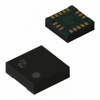
Connection Diagrams LMX2335U Thin Shrink Small Outline Package (TM) (Top View) LMX2336U Thin Shrink Small Outline Package (TM) (Top View) LMX2336U Ultra Thin Chip Scale Package (SLE) (Top View) LMX2335U Chip Scale Package (SLB) 10136702 LMX2336U Chip Scale Package (SLB) ...
Page 4
Pin Descriptions Pin No. Pin No. Pin No. Pin LMX2336U LMX2336U LMX2336U Name 20-Pin 20-Pin 24-Pin UTCSP TSSOP RF1 RF1 GND RF1 ...
Page 5
Pin Descriptions (Continued) Pin No. Pin No. Pin No. Pin LMX2336U LMX2336U LMX2336U Name 20-Pin 20-Pin 24-Pin UTCSP TSSOP CSP GND RF2 RF2 GND ...
Page 6
... Ordering Information Model Temperature Range LMX2335USLBX −40˚C to +85˚C LMX2335UTM −40˚C to +85˚C LMX2335UTMX −40˚C to +85˚C LMX2336USLEX −40˚C to +85˚C LMX2336USLBX −40˚C to +85˚C LMX2336UTM −40˚C to +85˚C LMX2336UTMX −40˚C to +85˚C www.national.com ...
Page 7
Detailed Block Diagram Notes supplies power to the RF1 and RF2 prescalers, RF1 and RF2 feedback dividers, RF1 and RF2 reference dividers, RF1 and RF2 phase detectors, the CC OSC buffer, MICROWIRE, and F LD circuits ...
Page 8
... Absolute Maximum Ratings Military/Aerospace specified devices are required, please contact the National Semiconductor Sales Office/ Distributors for availability and specifications. Power Supply Voltage V to GND CC V RF1 to GND P V RF2 to GND P Voltage on any pin to GND ( < V must be +6.5V I Storage Temperature Range (T ...
Page 9
Electrical Characteristics RF2 = 3.0V, −40˚C ≤ RF1 = Symbol Parameter RF1 SYNTHESIZER PARAMETERS ID RF1 RF1 Charge Pump Output Source o SOURCE Current ID RF1 RF1 Charge Pump Output Sink o ...
Page 10
Electrical Characteristics RF2 = 3.0V, −40˚C ≤ RF1 = Symbol Parameter RF2 SYNTHESIZER PARAMETERS ID RF2 RF2 Charge Pump Output Source o SOURCE Current ID RF2 RF2 Charge Pump Output Sink o ...
Page 11
Electrical Characteristics RF2 = 3.0V, −40˚C ≤ RF1 = Symbol Parameter PHASE NOISE CHARACTERISTICS L (f) RF1 RF1 Synthesizer Normalized Phase N Noise Contribution (Note 10) L(f) RF1 RF1 Synthesizer LMX2335U Single ...
Page 12
Electrical Characteristics RF2 = 3.0V, −40˚C ≤ RF1 = Symbol Parameter PHASE NOISE CHARACTERISTICS L (f) RF2 RF2 Synthesizer Normalized Phase N Noise Contribution (Note 10) L(f) RF2 RF2 Synthesizer LMX2335U Single ...
Page 13
Typical Performance Characteristics Sensitivity LMX2335U f RF1 Input Power Vs Frequency RF1 = 3. LMX2335U f RF1 Input Power Vs Frequency RF1 = 5. 10136746 10136747 www.national.com ...
Page 14
Typical Performance Characteristics Sensitivity (Continued) www.national.com LMX2336U f RF1 Input Power Vs Frequency RF1 = 3. LMX2336U f RF1 Input Power Vs Frequency RF1 = 5. 10136744 ...
Page 15
Typical Performance Characteristics Sensitivity (Continued) LMX2335U and LMX2336U f LMX2335U and LMX2336U f RF2 Input Power Vs Frequency RF2 = 3. RF2 Input Power Vs Frequency RF2 = 5.5V CC ...
Page 16
Typical Performance Characteristics Sensitivity (Continued) LMX2335U and LMX2336U OSC LMX2335U and LMX2336U OSC www.national.com Input Voltage Vs Frequency 3.0V CC Input Voltage Vs Frequency 5. 10136752 10136753 ...
Page 17
Typical Performance Characteristics Charge Pump LMX2335U and LMX2336U RF1 Charge Pump Sweeps −40˚C ≤ T ≤ +85˚ 10136760 www.national.com ...
Page 18
Typical Performance Characteristics Charge Pump (Continued) LMX2335U and LMX2336U RF2 Charge Pump Sweeps www.national.com −40˚C ≤ T ≤ +85˚ 10136761 ...
Page 19
Typical Performance Characteristics Input Impedance LMX2335U TSSOP and LMX2336U TSSOP f RF1 and f RF2 Input Impedance 3.0V +25˚ LMX2335U CSP and LMX2336U CSP f RF1 and f RF2 Input Impedance IN ...
Page 20
www.national.com 20 ...
Page 21
Typical Performance Characteristics Input Impedance (Continued) LMX2336U UTCSP f RF1 and f RF2 Input Impedance 3.0V +25˚ LMX2336U UTCSP f RF1 and 5.5V 10136797 21 ...
Page 22
www.national.com 22 ...
Page 23
Typical Performance Characteristics Input Impedance (Continued) LMX2335U TSSOP and LMX2336U TSSOP OSC Input Impedance Vs Frequency +25˚C A LMX2335U CSP and LMX2336U CSP OSC Input Impedance Vs Frequency +25˚ 10136776 10136777 www.national.com ...
Page 24
www.national.com 24 ...
Page 25
Typical Performance Characteristics Input Impedance (Continued) LMX2336U UTCSP OSC Input Impedance Vs Frequency +25˚ 101367A1 www.national.com ...
Page 26
www.national.com 26 ...
Page 27
Charge Pump Current Specification Definitions − ∆ Charge Pump Sink Current Charge Pump Sink Current ∆ Charge Pump Sink Current ...
Page 28
Test Setups LMX2335U and LMX2336U Charge Pump Test Setup The block diagram above illustrates the setup required to measure the LMX2336U device’s RF1 charge pump sink current. The same setup is used for the LMX2336TMEB/ LMX2336SLEEB Evaluation Boards. The RF2 ...
Page 29
Test Setups (Continued) LMX2335U and LMX2336U f The block diagram above illustrates the setup required to measure the LMX2336U device’s RF1 input sensitivity level. The same setup is used for the LMX2336TMEB/ LMX2336SLEEB Evaluation Boards. The RF2 input sensitiv- ity ...
Page 30
Test Setups (Continued) LMX2335U and LMX2336U OSC The block diagram above illustrates the setup required to measure the LMX2336U device’s OSC level. The same setup is used for the LMX2336TMEB/ LMX2336SLEEB Evaluation Boards. This setup is similar to the f ...
Page 31
Test Setups (Continued) LMX2335U and LMX2336U f The block diagram above illustrates the setup required to measure the LMX2336U device’s RF1 input impedance. The RF2 input impedance and reference oscillator impedance setups are very much similar. The same setup is ...
Page 32
LMX2335U and LMX2336U Serial Data Input Timing Notes: 1. Data is clocked into the 22-bit shift register on the rising edge of Clock 2. The MSB of Data is shifted in first. www.national.com 32 10136784 ...
Page 33
... Functional Description The basic phase-lock-loop (PLL) configuration consists of a high-stability crystal reference oscillator, a frequency synthe- sizer such as the National Semiconductor LMX2335U or LMX2336U, a voltage controlled oscillator (VCO), and a passive loop filter. The frequency synthesizer includes a phase detector, current mode charge pump, programmable reference R and feedback N frequency dividers ...
Page 34
Functional Description 1.5 PHASE/FREQUENCY DETECTORS The RF1 and RF2 phase/frequency detectors are driven from their respective N and R counter outputs. The maxi- mum frequency for both the RF1 and RF2 phase detector inputs is 10 MHz. The phase/frequency ...
Page 35
Functional Description 1.8.2 Open Drain FastLock Output The LMX233xU Fastlock feature allows faster loop response time during lock aquisition. The loop response time (lock time) can be approximately halved if the loop bandwidth is doubled. In order to achieve ...
Page 36
Programming Description 2.1 MICROWIRE INTERFACE The 22-bit shift register is loaded via the MICROWIRE interface. The shift register consists of a 20-bit Data[19:0] Field and a 2-bit Address[1:0] Field as shown below. The Address Field is used to decode ...
Page 37
37 www.national.com ...
Page 38
Programming Description 2.4 RF2 R REGISTER The RF2 R register contains the RF2 R_CNTR, PD_POL RF2, ID bits that compose the F LD control word. The detailed description and programming information for each control word is o discussed in ...
Page 39
Programming Description 2.4.4 TRI-STATE ID RF2 RF2 SYNTHESIZER CHARGE PUMP TRI-STATE CURRENT o The TRI-STATE ID RF2 bit allows the charge pump to be switched between a normal operating mode and a high impedance o output state. This happens ...
Page 40
Programming Description 2.5.4 PWDN RF2 RF2 SYNTHESIZER POWERDOWN The PWDN RF2 bit is used to switch the RF2 PLL between a powered up and powered down mode. Furthermore, the PWDN RF2 bit operates in conjuction with the TRI-STATE ID ...
Page 41
Programming Description 2.6.3 ID RF1 RF1 SYNTHESIZER CHARGE PUMP CURRENT GAIN o The ID RF1 bit controls the RF1 synthesizer’s charge pump gain. Two current levels are available. o Control Bit Register Location ID RF1 RF1 R[18] o 2.6.4 ...
Page 42
Programming Description 2.7.3 PRE RF1 RF1 SYNTHESIZER PRESCALER SELECT The RF1 synthesizer utilizes a selectable dual modulus prescaler. Control Bit Register Location PRE RF1 RF1 N[20] 2.7.4 PWDN RF1 RF1 SYNTHESIZER POWERDOWN The PWDN RF1 bit is used to ...
Page 43
Programming Description 2.8 F LD[3:0] MULTI-FUNCTION OUTPUT SELECT o The F LD control word is used to select which signal is routed to the LD3 F LD2 F LD1 F LD0 ...
Page 44
Physical Dimensions unless otherwise noted www.national.com inches (millimeters) 16-Pin Thin Shrink Small Outline Package (TM) NS Package Number MTC16 44 ...
Page 45
Physical Dimensions inches (millimeters) unless otherwise noted (Continued) 20-Pin Thin Shrink Small Outline Package (TM) NS Package Number MTC20 45 www.national.com ...
Page 46
Physical Dimensions www.national.com inches (millimeters) unless otherwise noted (Continued) 16-Pin Chip Scale Package (SLB) NS Package Number SLB16A 46 ...
Page 47
Physical Dimensions inches (millimeters) unless otherwise noted (Continued) 24-Pin Chip Scale Package (SLB) NS Package Number SLB24A 47 www.national.com ...
Page 48
... NATIONAL’S PRODUCTS ARE NOT AUTHORIZED FOR USE AS CRITICAL COMPONENTS IN LIFE SUPPORT DEVICES OR SYSTEMS WITHOUT THE EXPRESS WRITTEN APPROVAL OF THE PRESIDENT AND GENERAL COUNSEL OF NATIONAL SEMICONDUCTOR CORPORATION. As used herein: 1. Life support devices or systems are devices or systems which, (a) are intended for surgical implant ...