LMX2353SLBX National Semiconductor, LMX2353SLBX Datasheet
LMX2353SLBX
Specifications of LMX2353SLBX
LMX2353SLBXTR
Available stocks


Related parts for LMX2353SLBX


LMX2353SLBX Summary of contents
Page 1
... Functional Block Diagram Fastlock , MICROWIRE and PLLatinum are trademarks of National Semiconductor Corporation. ™ ™ ™ TRI-STATE ® registered trademark of National Semiconductor Corporation. © 2001 National Semiconductor Corporation Features n 2.7 V – 5.5 V operation n Low Current Consumption I = 5.5 mA typ Programmable or Logical Power Down Mode µ ...
Page 2
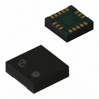
... Programmable CMOS output. Level of the output is controlled by F2[18] bit. — Programmable CMOS output. Level of the output is controlled by F2[17] bit. 2 DS101124-3 TOP VIEW Order Number LMX2353SLBX Description input CC ® charge ...
Page 3
... Absolute Maximum Ratings If Military/Aerospace specified devices are required, please contact the National Semiconductor Sales Office/ Distributors for availability and specifications. Power Supply Voltage Voltage on any pin with GND = Storage Temperature Range ( Lead Temperature (solder, 4 sec.) (T Electrical Characteristics All min/max specifications are guaranteed by design, or test, or statistical methods ...
Page 4
Electrical Characteristics All min/max specifications are guaranteed by design, or test, or statistical methods (Continued) Symbol Parameter MICROWIRE TIMING t Data to Clock Setup Time CS t Data to Clock Hold Time CH t Clock Pulse Width High CWH t ...
Page 5
Charge Pump Current Specification Definitions sink current CPo sink current CPo sink current CPo ...
Page 6
Typical Performance Characteristics LMX2353 Charge Pump Current vs CP Voltage O CP_WORD = 0011 and 1111 LMX2353 V Voltage vs V Load Current in V Doubler Mode www.national.com ...
Page 7
... The basic phase-lock-loop (PLL) configuration consists of a high-stability crystal reference oscillator, a frequency synthesizer such as the National Semiconductor LMX2353, a voltage controlled oscillator (VCO), and a passive loop filter. The frequency synthesizer includes a phase detector, current mode charge pump, as well as programmable reference [R] and feedback [N] frequency dividers ...
Page 8
Functional Description increased while maintaining the same frequency step size for channel selection. The division value N is thereby reduced giving a lower phase noise referred to the phase detector input, and the comparison frequency is increased allowing faster ...
Page 9
Functional Description 1 Multifunction Output O The F LD output pin can deliver several internal functions including analog/digital lock detects, and counter outputs. See o programming description 2.4.2 for more details. 1.8.1 Lock Detect Output A digital ...
Page 10
Programming Description (Continued) 2.1.2 Registers’ Truth Table www.national.com 10 ...
Page 11
Programming Description 2.2 R REGISTER If the ADDRESS[1:0] field is set data is transferred from the 24-bit shift register into the R register which sets the PLL’ s 15-bit R-counter divide ratio when Latch Enable (LE) ...
Page 12
Programming Description 2.2.4.2 Phase Detector Polarity (PD_POL) Depending upon VCO characteristics, the PD_POL (R_15) bit should be set accordingly: When VCO characteristics are positive like (1), PD_POL should be set HIGH; When VCO characteristics are negative like (2), PD_POL ...
Page 13
Programming Description 2.3.2.4 Power Down Mode (PWDN_MODE) Synchronous Power Down Mode The PLL loop can be synchronously powered down by setting the PWDN mode bit HIGH (F2_19=1) and then asserting the power down mode bit (N20 = 1). The ...
Page 14
Programming Description R: Preset divide ratio of binary 15-bit programmable reference counter (3 to 32767) P: Preset modulus of dual modulus prescaler ( 32) 2.4 F1 REGISTER If the ADDRESS[1:0] field is set ...
Page 15
Programming Description 2.4.2.3 Analog Lock Detect Filter When the F LD output is configured as analog lock detect output, an external lock detect circuit is needed in order to provide a O steady LOW signal when the PLL is ...
Page 16
Programming Description 2.4.2.4 Typical Lock Detecting Timing 2.5 F2 REGISTER If the ADDRESS[1:0] field is set data is transferred from the 24-bit shift register into the F2 register when Latch Enable (LE) signal goes high. The ...
Page 17
Programming Description The low gain or steadystate mode for fastlocking is defined to be whenever the charge pump current selected is less than 900 µA. The high gain or acquisition mode is defined to be whenever the charge pump ...
Page 18
Physical Dimensions www.national.com inches (millimeters) unless otherwise noted TSSOP Package For Tube Quantity (94 Units Per Tube) For Tape and Reel (2500 Units Per Reel) Order Number LMX2353TM or LMX2353TMX NS Package Number MTC16 18 ...
Page 19
... National does not assume any responsibility for use of any circuitry described, no circuit patent licenses are implied and National reserves the right at any time without notice to change said circuitry and specifications. inches (millimeters) unless otherwise noted (Continued) Chip Scale Package For Tape and Reel (2500 Units Per Reel) Order Number: LMX2353SLBX NS Package Number SLB16A 2. A critical component is any component of a life support device or system whose failure to perform ...