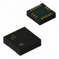
LMX2353SLBX National Semiconductor, LMX2353SLBX Datasheet - Page 16

LMX2353SLBX
Manufacturer Part Number
LMX2353SLBX
Description
IC FREQ SYNTH 2.5GHZ 16LAMCSP
Manufacturer
National Semiconductor
Series
PLLatinum™r
Type
PLL Frequency Synthesizerr
Datasheet
1.LMX2353TMNOPB.pdf
(19 pages)
Specifications of LMX2353SLBX
Pll
Yes with Bypass
Input
CMOS, TTL
Output
CMOS
Number Of Circuits
1
Ratio - Input:output
2:1
Differential - Input:output
Yes/No
Frequency - Max
2.5GHz
Divider/multiplier
Yes/Yes
Voltage - Supply
2.7 V ~ 5.5 V
Operating Temperature
-40°C ~ 85°C
Mounting Type
Surface Mount
Package / Case
16-Laminate CSP
Frequency-max
2.5GHz
Lead Free Status / RoHS Status
Lead free / RoHS Compliant
Other names
LMX2353SLBX/NOPB
LMX2353SLBXTR
LMX2353SLBXTR
Available stocks
Company
Part Number
Manufacturer
Quantity
Price
Company:
Part Number:
LMX2353SLBX
Manufacturer:
ON
Quantity:
100
www.national.com
Most Significant Bit
_21
23
F2
0
2.0 Programming Description
2.4.2.4 Typical Lock Detecting Timing
2.5 F2 REGISTER
If the ADDRESS[1:0] field is set to 0 1, data is transferred from the 24-bit shift register into the F2 register when Latch Enable (LE)
signal goes high. The F2 register sets the CMOS output word bit CMOS[3:0] and the power down mode bit PWDN_MODE. The
rest of the bits F2_0 - F2_14, and F2_20-F_21 are Don’t Care.
Note:0 denotes setting the bit to zero
2.5.1 PWDN_MODE (F2_19)
See section 2.3.2 describing the control word and power down.
2.5.2 Programmable CMOS Outputs (F2_15–F2_18)
2.5.3 OUT0/OUT1 Truth Table
The CMOS[3:0] 4-bit register selects one of three modes for the OUT_0 and OUT_1 pins. The OUT_0 and OUT_1 pins are
normally used as general purpose CMOS outputs or as part of a Fastlock
overrides the other two normal modes when activated.
GENERAL PURPOSE CMOS OUTPUT MODE: The general purpose CMOS output mode is selected when the Fastlock
(F2_F18) and TEST bit (F2_17) are set LOW. The logic levels of the OUT_0 bit (F2_15) and OUT_1 bit (F2_16) then determine
the logic states of the OUT_0 and OUT_1 pins.
Fastlock
Fastlock
momentarily while acquiring lock by increasing the charge pump output current magnitude while simultaneously switching in a
second resistor element to ground via the OUT0 output pin.
_20
F2
22
FastLock
0
OUT_0
OUT_1
TEST
FastLock
Bit
F2_18
™
™
PWDN_
MODE
_19
mode is selected when the Fastlock
MODE: The Fastlock bit (F2_18) selects between the general purpose CMOS output or Fastlock
21
F2
_18
20
F2
Location
CMOS[3:0]
_17
F2_15
F2_16
F2_17
F2_18
19
F2
_16
F2
18
F2_17
TEST
_15
17
F2
Set the output logic level of
Set the output logic level of
_14
F2
16
™
_13
FastLock Mode
15
F2
bit is HIGH. The Fastlock
Data Field
Function
OUT0 pin
OUT1 pin
(Continued)
_12
Test
14
F2
OUT_1
SHIFT REGISTER BIT LOCATION
F2_16
_11
F2
13
These bits should be set to zero
16
_10
12
F2
11 10
F2
_9
™
™
F2
_8
mode allows the user to open up the loop bandwidth
scheme. There is also a production test mode that
OUT_0
CMOS Output Mode
F2_15
F2
_7
9
Normal Operation
F2
_6
8
LOW
LOW
0
F2
_5
7
F2
_4
6
F2
_3
5
F2
_2
4
F2
_1
3
Least Significant Bit
FastLock Mode
Test Mode
F2
_0
2
™
DS101124-7
HIGH
HIGH
1
modes. The
Address Field
1
0
™
bit
0
0


