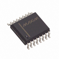
DS1023S-50+ Maxim Integrated Products, DS1023S-50+ Datasheet - Page 13

DS1023S-50+
Manufacturer Part Number
DS1023S-50+
Description
IC TIMING ELEMENT PROG 16-SOIC
Manufacturer
Maxim Integrated Products
Datasheet
1.DS1023S-25.pdf
(16 pages)
Specifications of DS1023S-50+
Number Of Taps/steps
256
Function
1-Shot
Delay To 1st Tap
16.5nS
Tap Increment
0.5nS
Available Total Delays
127.5ns
Voltage - Supply
4.75 V ~ 5.25 V
Operating Temperature
0°C ~ 70°C
Mounting Type
Surface Mount
Package / Case
16-SOIC (0.300", 7.5mm Width)
Propagation Delay Time
0.5 ns
Supply Voltage (min)
4.75 V
Operating Temperature Range
0 C to + 70 C
High Level Output Current
- 1 mA
Interface
Serial, Parallel
Logic Type
CMOS, TTL
Low Level Output Current
8 mA
Maximum Operating Temperature
+ 70 C
Minimum Operating Temperature
0 C
Mounting Style
SMD/SMT
Supply Voltage (max)
5.25 V
Lead Free Status / RoHS Status
Lead free / RoHS Compliant
Number Of Independent Delays
-
Lead Free Status / Rohs Status
Lead free / RoHS Compliant
NOTES:
1. Delay from input to output with a programmed delay value of zero.
2. This is the relative delay between REF and OUT. The device is trimmed such that when programmed
3. The reference delay is closely matched to the step zero delay to allow relative timings down to zero or
4. This is the worst case condition when the SubDAC switches from its maximum to minimum value.
5. This is the actual measured delay from IN to OUT. This parameter will exhibit greater temperature
6. This is the actual measured delay with respect to the REF output. This parameter more closely
7. This is the maximum deviation from a straight line response drawn between the step zero delay and
8. Change in delay value when the inverted output is selected instead of the normal, non-inverting,
9. In PWM mode the delay between the rising edge of the input and the rising edge of the output.
10. The minimum value for which the PWM pulse width should be programmed. Narrower pulse widths
11. This is the minimum allowable interval between transitions on the input to assure accurate device
12. This parameter applies to normal delay mode only. When a 50% duty cycle input clock is used this
13. Measured from rising edge of the input to the rising edge of the output (t
14. From rising edge to rising edge.
15. Faster rise and fall times will give the greatest accuracy in measured delay. Slow edges (outside the
16. Min and max limits do not apply for steps 253-255. Only the typical value applies for those steps.
to zero delay the OUT output will always appear before the REF output.
numerically equal to t
less.
All other steps are ±0.5 lsb. This comment does not apply to -200 and -500 devices which do not use
a SubDAC. (See Figure 14)
variation than the relative delay parameter.
reflects the programmed delay value than the absolute delay parameter. (See Figure 15).
the maximum programmed delay. Therefore it is indicative of the maximum error in the measured
delay versus the programmed delay with respect to the REF output. The absolute delay measurement
from IN to OUT will in addition have an offset error equal to the step zero delay and its tolerance.
(See Figure 13).
output.
may be programmed but output levels may be impaired and ultimately no output pulse will be
produced.
operation. This parameter may be violated but timing accuracy may be impaired and ultimately very
narrow pulse widths will result in no output from the device.
defines the highest usable clock frequency. When asymmetrical clock inputs are used the maximum
usable clock frequency must be reduced to conform to the minimum input pulse width requirement. In
PWM mode the minimum input period is equal to the step zero delay and the programmed delay
(t
specification maximum) may result in erratic operations.
DO
+ t
D
).
D0
-t
REF
. (See Figure 15).
13 of 16
DR
).
This parameter is


