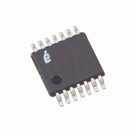
X1288V14T1 Intersil, X1288V14T1 Datasheet - Page 13

X1288V14T1
Manufacturer Part Number
X1288V14T1
Description
IC RTC/CAL/CPU SUP EE 14-TSSOP
Manufacturer
Intersil
Type
Clock/Calendar/Supervisor/EEPROMr
Datasheet
1.X1288S16.pdf
(27 pages)
Specifications of X1288V14T1
Memory Size
256K (32K x 8)
Time Format
HH:MM:SS:hh (12/24 hr)
Date Format
YY-MM-DD-dd
Interface
I²C, 2-Wire Serial
Voltage - Supply
4.5 V ~ 5.5 V
Operating Temperature
-40°C ~ 85°C
Mounting Type
Surface Mount
Package / Case
14-TSSOP
Lead Free Status / RoHS Status
Contains lead / RoHS non-compliant
CONTROL REGISTERS
The Control Bits and Registers, described under this
section, are nonvolatile.
Block Protect Bits - BP2, BP1, BP0
The Block Protect Bits, BP2, BP1 and BP0, determine
which blocks of the array are write protected. A write to a
protected block of memory is ignored. The block protect
bits will prevent write operations to one of eight segments
of the array. The partitions are described in Table 3.
Watchdog Timer Control Bits - WD1, WD0
The bits WD1 and WD0 control the period of the
Watchdog Timer. See Table 4 for options.
Table 3. Block Protect Bits
Table 4. Watchdog Timer Time-Out Options
INTERRUPT CONTROL AND FREQUENCY
OUTPUT REGISTER (INT)
Interrupt Control and Status Bits (IM, AL1E, AL0E)
There are two Interrupt Control bits, Alarm 1 Interrupt
Enable (AL1E) and Alarm 0 Interrupt Enable (AL0E) to
specifically enable or disable the alarm interrupt signal
output (IRQ). The interrupts are enabled when either
AL1E and AL0E are set to ‘1’, respectively.
Two volatile bits (AL1 and AL0), associated with the
two alarms respectively, indicate if an alarm has hap-
pened. These bits are set on an alarm condition
regardless of whether the IRQ interrupt is enabled.
WD1 WD0
0
0
0
0
1
1
1
1
0
0
1
1
0
0
1
1
0
0
1
1
0
1
0
1
0
1
0
1
0
1
0
1
6000h – 7FFFh
4000h – 7FFFh
0000h – 7FFFh
0000h – 007Fh
0000h – 00FFh
0000h – 01FFh
0000h – 03FFh
Watchdog Time-Out Period
Addresses
Protected
X1288
None
Disabled (default)
13
750 milliseconds
250 milliseconds
1.75 seconds
None (default)
Array Lock
First 2 pgs
First 4 pgs
First 8 Pgs
First Page
Upper 1/4
Upper 1/2
Full Array
X1288
The AL1 and AL0 bits in the status register are reset
by the falling edge of the eighth clock of a read of the
register containing the bits.
Pulse Interrupt Mode
The pulsed interrupt mode allows for repetitive or
recurring alarm functionality. Hence an repetitive or
recurring alarm can be set for every n
minute, or n
the week. The pulsed interrupt mode can be consid-
ered a repetitive interrupt mode, with the repetition
rate set by the time setting fo the alarm.
The Pulse Interrupt Mode is enabled when the IM bit is
set.
The Alarm IRQ output will output a single pulse of
short duration (approximately 10-40ms) once the
alarm condition is met. If the interrupt mode bit (IM bit)
is set, then this pulse will be periodic.
Programmable Frequency Output Bits - FO1, FO0
These are two output control bits. They select one of
three divisions of the internal oscillator, that is applied
to the PHZ output pin. Table 5 shows the selection bits
for this output. When using the PHZ output function,
the Alarm IRQ output function is disabled.
Table 5. Programmable Frequency Output Bits
ON-CHIP OSCILLATOR COMPENSATION
Digital Trimming Register (DTR) - DTR2, DTR1 and
DTR0 (Non-Volatile)
The digital trimming Bits DTR2, DTR1 and DTR0
adjust the number of counts per second and average
the ppm error to achieve better accuracy.
DTR2 is a sign bit. DTR2=0 means frequency
compensation is > 0. DTR2=1 means frequency
compensation is < 0.
DTR1 and DTR0 are scale bits. DTR1 gives 10 ppm
adjustment and DTR0 gives 20 ppm adjustment.
A range from -30ppm to +30ppm can be represented
by using three bits above.
IM Bit
FO1
0
0
1
1
0
1
FO0
Single Time Event Set By Alarm
Repetitive/Recurring Time Event Set By Alarm
0
1
0
1
th
hour, or n
Interrupt/Alarm Frequency
(average of 100 samples)
th
Output Frequency
Alarm IRQ output
date, or for the same day of
32.768kHz
100Hz
1Hz
th
second, or n
April 14, 2006
FN8102.3
th


