DS1603+ Maxim Integrated Products, DS1603+ Datasheet - Page 2
DS1603+
Manufacturer Part Number
DS1603+
Description
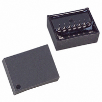
IC COUNTER ELAPSED TIME 5V 7-SIP
Manufacturer
Maxim Integrated Products
Type
Elapsed Time Counterr
Datasheet
1.DS1603.pdf
(9 pages)
Specifications of DS1603+
Time Format
Binary
Date Format
Binary
Interface
3-Wire Serial
Voltage - Supply
4.5 V ~ 5.5 V
Operating Temperature
0°C ~ 70°C
Mounting Type
Through Hole
Package / Case
14-DIP Module
Lead Free Status / RoHS Status
Lead free / RoHS Compliant
Memory Size
-


DS1603
With
at high level 8 bits are loaded into the protocol shift register providing read/write, register
RST
select, register clear, and oscillator trim information. Each bit is serially input on the rising edge of the
clock input. After the first eight clock cycles have loaded the protocol register with a valid protocol
additional clocks will output data for a read or input data for a write. V
must be present to access the
CC
DS1603. If V
< V
, the DS1603 will switch to internal power and disable the serial port to conserve
CC
TP
energy. When running off of the internal power supply, only the continuous counter will continue to
count and the counter powered by V
will stop, but retain the count, which had accumulated when V
CC
CC
power was lost. The 32-bit V
counter is gated by V
and the internal 1Hz signal.
CC
CC
PROTOCOL REGISTER
The protocol bit definition is shown in Figure 2. Valid protocols and the resulting actions are shown in
Table 1. Each data transfer to the protocol register designates what action is to occur. As defined, the
MSB (bit 7 which is designated ACC) selects the 32-bit continuous counter for access. If ACC is a logical
1 the continuous counter is selected and the 32 clock cycles that follow the protocol will either read or
write this counter. If the counter is being read, the contents will be latched into a different register at the
end of protocol and the latched contents will be read out on the next 32 clock cycles. This avoids reading
garbled data if the counter is clocked by the oscillator during a read. Similarly, if the counter is to be
written, the data is buffered in a register and all 32 bits are jammed into the counter simultaneously on the
nd
rising edge of the 32
clock. The next bit (bit 6 which is designated AVC) selects the 32–bit V
active
CC
counter for access. If AVC is a logical 1 this counter is selected and the 32 clock cycles that follow will
either read or write this counter. If both bit 7 and bit 6 are written to a logic high, all clock cycles beyond
the protocol are ignored and bit 5, 4, and 3 are loaded into the oscillator trim register. A value of binary 3
(011) will give a clock accuracy of
120 seconds per month at +25 C. Increasing the binary number
towards 7 will cause the real- time clock to run faster. Conversely, lowering the binary number towards 0
will cause the clock to run slower. Binary 000 will stop the oscillator completely. This feature can be used
to conserve battery life during storage. In this mode the internal power supply current is reduced to 100
nA maximum. In applications where oscillator trimming is not practical or not needed, a default setting of
011 is recommended. Bit 2 of protocol (designated CCC) is used to clear the continuous counter. When
set to logic 1, the continuous counter will reset to 0 when
is taken low. Bit 1 of protocol (designated
RST
CVC) is used to clear the V
active counter. When set to logical 1, the V
active counter will reset to 0
CC
CC
when
is taken low. Both counters can be reset simultaneously by setting CCC and CVC both to a
RST
logical 1. Bit 0 of the protocol (designated RD) determines whether the 32 clocks to follow will write a
counter or read a counter. When RD is set to a logical 0 a write action will follow when RD is set to a
logical 1 a read action will follow. When sending the protocol, 8 bits should always be sent. Sending less
than 8 bits can produce erroneous results. If clearing the counters or trimming the oscillator, the data
transfer can be terminated after the 8-bit protocol is sent. However, when reading or writing the counters,
32 clock cycles should always follow the protocol.
RESET AND CLOCK CONTROL
All data transfers are initiated by driving the
input high. The
input has two functions. First,
RST
RST
turns on the serial port logic, which allows access to the protocol register for the protocol data entry.
RST
Second, the
signal provides a method of terminating the protocol transfer or the 32-bit counter
RST
transfer. A clock cycle is a sequence of a rising edge followed by a falling edge. For write inputs, data
must be valid during the rising edge of the clock. Data bits are output on the falling edge of the clock
when data is being read. All data transfers terminate if the
input is transitioned low and the DQ pin
RST
goes to a high- impedance state.
should only be transitioned low while the clock is high to avoid
RST
disturbing the last bit of data. All data transfers must consist of 8 bits when transferring protocol only or
8 + 32 bits when reading or writing either counter. Data transfer is illustrated in Figure 3.
2 of 9
Related parts for DS1603+
Image
Part Number
Description
Manufacturer
Datasheet
Request
R

Part Number:
Description:
MAX7528KCWPMaxim Integrated Products [CMOS Dual 8-Bit Buffered Multiplying DACs]
Manufacturer:
Maxim Integrated Products
Datasheet:
Part Number:
Description:
Single +5V, fully integrated, 1.25Gbps laser diode driver.
Manufacturer:
Maxim Integrated Products
Datasheet:
Part Number:
Description:
Single +5V, fully integrated, 155Mbps laser diode driver.
Manufacturer:
Maxim Integrated Products
Datasheet:
Part Number:
Description:
VRD11/VRD10, K8 Rev F 2/3/4-Phase PWM Controllers with Integrated Dual MOSFET Drivers
Manufacturer:
Maxim Integrated Products
Datasheet:
Part Number:
Description:
Highly Integrated Level 2 SMBus Battery Chargers
Manufacturer:
Maxim Integrated Products
Datasheet:
Part Number:
Description:
Current Monitor and Accumulator with Integrated Sense Resistor; ; Temperature Range: -40°C to +85°C
Manufacturer:
Maxim Integrated Products
Part Number:
Description:
TSSOP 14/A�/RS-485 Transceivers with Integrated 100O/120O Termination Resis
Manufacturer:
Maxim Integrated Products
Part Number:
Description:
TSSOP 14/A�/RS-485 Transceivers with Integrated 100O/120O Termination Resis
Manufacturer:
Maxim Integrated Products
Part Number:
Description:
QFN 16/A�/AC-DC and DC-DC Peak-Current-Mode Converters with Integrated Step
Manufacturer:
Maxim Integrated Products
Part Number:
Description:
TDFN/A/65V, 1A, 600KHZ, SYNCHRONOUS STEP-DOWN REGULATOR WITH INTEGRATED SWI
Manufacturer:
Maxim Integrated Products
Part Number:
Description:
Integrated Temperature Controller f
Manufacturer:
Maxim Integrated Products
Part Number:
Description:
SOT23-6/I�/45MHz to 650MHz, Integrated IF VCOs with Differential Output
Manufacturer:
Maxim Integrated Products
Part Number:
Description:
SOT23-6/I�/45MHz to 650MHz, Integrated IF VCOs with Differential Output
Manufacturer:
Maxim Integrated Products
Part Number:
Description:
EVALUATION KIT/2.4GHZ TO 2.5GHZ 802.11G/B RF TRANSCEIVER WITH INTEGRATED PA
Manufacturer:
Maxim Integrated Products
Part Number:
Description:
QFN/E/DUAL PCIE/SATA HIGH SPEED SWITCH WITH INTEGRATED BIAS RESISTOR
Manufacturer:
Maxim Integrated Products
Datasheet: