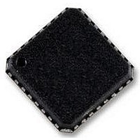
AD7195BCPZ Analog Devices Inc, AD7195BCPZ Datasheet - Page 40

AD7195BCPZ
Manufacturer Part Number
AD7195BCPZ
Description
IC AFE 24BIT 4.8K 32LFSP
Manufacturer
Analog Devices Inc
Datasheet
1.AD7195BCPZ-RL.pdf
(44 pages)
Specifications of AD7195BCPZ
Design Resources
Precision Weigh Scale Design Using AD7195 with Internal PGA and AC Excitation (CN0155)
Number Of Bits
24
Number Of Channels
4
Voltage - Supply, Analog
4.75 V ~ 5.25 V
Voltage - Supply, Digital
2.7 V ~ 5.25 V
Package / Case
32-LFCSP
Resolution (bits)
24bit
Sampling Rate
4.8kSPS
Input Channel Type
Pseudo Differential
Data Interface
3-Wire, Serial
Supply Voltage Range - Analog
4.75V To 5.25V
Lead Free Status / RoHS Status
Lead free / RoHS Compliant
Power (watts)
-
Lead Free Status / RoHS Status
Lead free / RoHS Compliant, Lead free / RoHS Compliant
Available stocks
Company
Part Number
Manufacturer
Quantity
Price
Company:
Part Number:
AD7195BCPZ
Manufacturer:
Analog Devices Inc
Quantity:
135
Company:
Part Number:
AD7195BCPZ
Manufacturer:
TST
Quantity:
5 000
Part Number:
AD7195BCPZ
Manufacturer:
ADI/亚德诺
Quantity:
20 000
Company:
Part Number:
AD7195BCPZ-RL
Manufacturer:
SEMTECH
Quantity:
394
AD7195
CHOP ENABLED (SINC
With chop enabled, the ADC offset and offset drift are
minimized. The analog input pins are continuously swapped.
With the analog input pins connected in one direction, the
settling time of the sinc filter is allowed and a conversion is
recorded. The analog input pins invert and another settled
conversion is obtained. Subsequent conversions are averaged
to minimize the offset. This continuous swapping of the analog
input pins and the averaging of subsequent conversions means
that the offset drift is also minimized. With chop enabled, the
resolution increases by 0.5 bits. Using the sinc
enabled is suitable for output data rates up to 320 Hz.
Output Data Rate and Settling Time (Sinc
Enabled)
For the sinc
where:
f
f
FS[9:0] is the decimal equivalent of Bit FS9 to Bit FS0 in the
mode register.
The value of FS[9:0] can be varied from 1 to 1023. This results
in an output data rate of 1.56 Hz to 1600 Hz. The settling time
is equal to
Table 34. Examples of Output Data Rates and the
Corresponding Settling Time (Chop Enabled, Sinc
FS[9:0]
96
80
When a channel change occurs, the modulator and filter are
reset. The complete settling time is required to generate the first
conversion after the channel change. Subsequent conversions on
this channel occur at 1/f
ADC
CLK
CONVERSIONS
is the master clock (4.92 MHz nominal).
is the output data rate.
f
t
ADC
SETTLE
CHANNEL
= f
= 2/f
3
CLK
Output Data Rate (Hz)
16.7
20
Figure 46. Channel Change (Sinc
Figure 45. Chop Enabled (Sinc
filter, the output data rate is equal to
/(3 × 1024 × FS[9:0])
CH A
ADC
CHOP
CHANNEL A
CH A CH A
ADC
MODULATOR
.
3
FILTER)
ADC
1/
3
CH B
Chop Enabled)
f
CHANNEL B
ADC
3
Chop Enable)
Settling Time (ms)
120
100
CH B
SINC
3
3
filter with chop
3
CH B
Chop
/SINC
CH B
4
3
Filter)
CH B
Rev. 0 | Page 40 of 44
If conversions are performed on a single channel and a step
change occurs, the ADC does not detect the change in analog
input; therefore, it continues to output conversions at the
programmed output data rate. However, it is at least two
conversions later before the output data accurately reflects
the analog input. If the step change occurs while the ADC is
processing a conversion, then the ADC takes three conversions
after the step change to generate a fully settled result.
The cutoff frequency f
50 Hz/60 Hz Rejection (Sinc
When FS[9:0] is set to 96 and chopping is enabled, the filter
response shown in Figure 48 is obtained. The output data rate
is equal to 16.7 Hz for a 4.92 MHz master clock. The chopping
introduces notches at odd integer multiples of f
notches due to the sinc filter in addtion to the notches intro-
duced by the chopping means that simultaneous 50 Hz and
60 Hz rejection is achieved for an output data rate of 16.7 Hz.
The rejection at 50 Hz/60 Hz ± 1 Hz is typically 53 dB,
assuming a stable master clock.
Figure 47. Asynchronous Step Change in Analog Input (Sinc
f
–100
–110
–120
3dB
–10
–20
–30
–40
–50
–60
–70
–80
–90
Figure 48. Sinc
ANALOG
OUTPUT
0
= 0.24 × f
0
INPUT
ADC
25
ADC
3
Filter Response (FS[9:0] = 96, Chop Enabled)
3dB
1/
f
50
ADC
is equal to
FREQUENCY (Hz)
3
Chop Enabled)
75
100
SETTLED
FULLY
ADC
125
3
/2. The
Chop Enabled)
150


