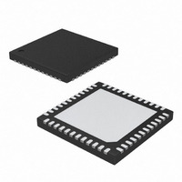
MAX5865ETM+T Maxim Integrated Products, MAX5865ETM+T Datasheet - Page 17

MAX5865ETM+T
Manufacturer Part Number
MAX5865ETM+T
Description
IC ANLG FRONT END 40MSPS 48-TQFN
Manufacturer
Maxim Integrated Products
Datasheet
1.MAX5865ETM.pdf
(26 pages)
Specifications of MAX5865ETM+T
Number Of Bits
10
Number Of Channels
4
Power (watts)
2.10W
Voltage - Supply, Analog
2.7 V ~ 3.3 V
Voltage - Supply, Digital
1.8 V ~ 3.3 V
Package / Case
48-TQFN Exposed Pad
Lead Free Status / RoHS Status
Lead free / RoHS Compliant
Shutdown mode offers the most dramatic power sav-
ings by shutting down all the analog sections of the
MAX5865 and placing the ADCs’ digital outputs in tri-
state mode. When the ADCs’ outputs transition from tri-
state to on, the last converted word is placed on the
digital outputs. The DACs’ digital bus inputs must be
zero or OV
up. The DACs’ previously stored data is lost when com-
ing out of shutdown mode. The wake-up time from shut-
down mode is dominated by the time required to
charge the capacitors at REFP, REFN, and COM. In
internal reference mode and buffered external refer-
ence mode, the wake-up time is typically 40µs to enter
Xcvr mode, 20µs to enter Rx mode, and 40µs to enter
Tx MODE.
In idle mode, the reference and clock distribution cir-
cuits are powered, but all other functions are off. The
ADCs’ outputs are forced to tri-state. The DACs’ digital
bus inputs must be zero or OV
not internally pulled up. The wake-up time from the idle
mode is 10µs required for the ADCs and DACs to be
fully operational. When the ADCs’ outputs transition
from tri-state to on, the last converted word is placed
on the digital outputs. In the idle mode, the supply cur-
Table 3. MAX5865 Operation Modes
X = Don’t care.
QSPI is a trademark of Motorola, Inc.
FUNCTION
Shutdown
Standby
Xcvr
Idle
Rx
Tx
DD
because the bus is not internally pulled
D evi ce shutd ow n. RE F i s off, AD C s ar e
off, and the AD C b us i s tr i - stated ; D AC s
ar e off and the D AC i np ut b us m ust b e
set to zer o or OV
REF and CLK are on, ADCs are off,
and the ADC bus is tri-stated; DACs
are off and the DAC input bus must be
set to zero or OV
REF is on, ADCs are on; DACs are off,
and the DAC input bus must be set to
zero or OV
REF is on, ADCs are off, and the ADC
bus is tri-stated; DACs are on.
REF is on, ADCs and DACs are on.
REF is on, ADCs are off, and the ADC
bus is tri-stated; DACs are off and the
DAC input bus must be set to zero or
OV
______________________________________________________________________________________
DD
Performance, 40Msps Analog Front End
.
DD
DESCRIPTION
.
D D
DD
DD
.
.
, because the bus is
Ultra-Low-Power, High-Dynamic-
(MSB)
D7
X
X
X
X
X
X
rent is lowered if the clock input is set to zero or OV
however, the wake-up time extends to 40µs.
In standby mode, only the ADCs’ reference is powered;
the rest of the device’s functions are off. The pipeline
ADCs are off and DA0 to DA7 are in tri-state mode. The
DACs’ digital bus inputs must be zero or OV
because the bus is not internally pulled up. The wake-
up time from standby mode to the Xcvr mode is domi-
nated by the 40µs required to activate the pipeline
ADCs and DACs. When the ADC outputs transition from
tri-state to active, the last converted word is placed on
the digital outputs.
The serial digital interface is a standard 3-wire connec-
tion compatible with SPI/QSPI™/MICROWIRE/DSP
interfaces. Set CS low to enable the serial data loading
at DIN. Following CS high-to-low transition, data is shift-
ed synchronously, MSB first, on the rising edge of the
serial clock (SCLK). After 8 bits are loaded into the seri-
al input register, data is transferred to the latch. CS
must transition high for a minimum of 80ns before the
next write sequence. The SCLK can idle either high or
low between transitions.
timing diagram of the 3-wire serial interface.
D6
X
X
X
X
X
X
D5
X
X
X
X
X
X
D4
X
X
X
X
X
X
D3
Figure 5
X
X
X
X
X
X
D2
0
0
0
0
1
1
shows the detailed
D1
0
0
1
1
0
0
D0
0
1
0
1
0
1
DD
DD
17
;


