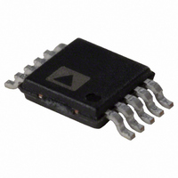
AD7992BRMZ-1 Analog Devices Inc, AD7992BRMZ-1 Datasheet - Page 24

AD7992BRMZ-1
Manufacturer Part Number
AD7992BRMZ-1
Description
IC ADC 12BIT 2CHAN I2C 10-MSOP
Manufacturer
Analog Devices Inc
Datasheet
1.AD7992BRMZ-1.pdf
(28 pages)
Specifications of AD7992BRMZ-1
Data Interface
I²C, Serial
Operating Temperature
-40°C ~ 125°C
Number Of Bits
12
Sampling Rate (per Second)
79k
Number Of Converters
1
Power Dissipation (max)
2.2mW
Voltage Supply Source
Single Supply
Mounting Type
Surface Mount
Package / Case
10-TFSOP (0.118", 3.00mm Width)
Resolution (bits)
12bit
Input Channel Type
Single Ended
Supply Voltage Range - Analogue
2.7V To 5.5V
Supply Current
1.4mA
No. Of Pins
10
Sampling Rate
188kSPS
Rohs Compliant
Yes
Lead Free Status / RoHS Status
Lead free / RoHS Compliant
For Use With
EVAL-AD7992CB - BOARD EVALUATION FOR AD7992
Lead Free Status / RoHS Status
Lead free / RoHS Compliant
Available stocks
Company
Part Number
Manufacturer
Quantity
Price
Part Number:
AD7992BRMZ-1
Manufacturer:
ADI/亚德诺
Quantity:
20 000
AD7992
ALERT/BUSY PIN
The ALERT/BUSY pin may be configured as an ALERT output
or BUSY output, as shown in Table 11.
SMBus ALERT
The AD7992 ALERT output is an SMBus interrupt line for
devices that want to trade their ability to master for an extra
pin. The AD7992 is a slave-only device and uses the SMBus
ALERT to signal the host device that it wants to talk. The
SMBus ALERT on the AD7992 is used as an out-of-conversion-
range indicator (a limit violation indicator).
The ALERT pin has an open-drain configuration that allows the
ALERT outputs of several AD7992s to be wire-AND’ e d together
when the ALERT pin is active low. D0 of the configuration
register is used to set the active polarity of the ALERT output.
The power-up default is active low. The ALERT function can be
disabled or enabled by setting D2 of the configuration register
to 0 or 1, respectively.
The host device can process the ALERT interrupt and simul-
taneously access all SMBus ALERT devices through the alert
response address. Only the device that pulled the ALERT low
acknowledges the ARA (alert response address). If more than
one device pulls the ALERT pin low, the highest priority (lowest
address) device wins communication rights via standard I
arbitration during the slave address transfer.
The ALERT output becomes active when the value in the
conversion result register exceeds the value in the DATA
register or falls below the value in the DATA
selected channel. It is reset when a write operation to the
configuration register sets D1 to a 1, or when the conversion
result returns N LSBs below or above the value stored in the
DATA
value in the hysteresis register (see the Limit Registers section).
HIGH
register or DATA
SDA
SCL
START BY
MASTER
0
1
LOW
0
register, respectively. N is the
HS-MODE MASTER CODE
0
FAST MODE
0
LOW
1
register for a
Figure 30. Placing the Part into High Speed Mode
X
X
HIGH
2
C
X
Rev. 0 | Page 24 of 28
NACK
9
Sr
1
The ALERT output requires an external pull-up resistor that
can be connected to a voltage different from V
maximum voltage rating of the ALERT output pin is not
exceeded. The value of the pull-up resistor depends on the
application, but should be as large as possible to avoid excessive
sink currents at the ALERT output.
PLACING THE AD7992-1 INTO HIGH SPEED MODE
High speed mode communication commences after the master
addresses all devices connected to the bus with the master code,
00001XXX, to indicate that a high speed mode transfer is to
begin. No device connected to the bus is allowed to acknowl-
edge the high speed master code; therefore, the code is followed
by a not acknowledge (see Figure 30). The master must then
issue a repeated start followed by the device address with a R/ W
bit. The selected device then acknowledges its address.
All devices continue to operate in high speed mode until the
master issues a STOP condition. When the STOP condition is
issued, the devices all return to fast mode.
THE ADDRESS SELECT (AS) PIN
The address select pin on the AD7992 is used to set the I
address for the AD7992 device. The AS pin can be tied to V
to AGND, or left floating. The selection should be made as close
as possible to the AS pin; avoid having long tracks introducing
extra capacitance onto the pin. This is important for the float
selection, because the AS pin has to charge to a midpoint after
the start bit during the first address byte. Extra capacitance on
the AS pin increases the time taken to charge to the midpoint
and may cause an incorrect decision on the device address.
When the AS pin is left floating, the AD7992 can work with a
capacitive load up to 40 pF.
0
1
SERIAL BUS ADDRESS BYTE
HIGH SPEED MODE
0
A3
A2
A1
A0
ACK. BY
AD7992
9
DD
provided the
2
C
DD
,


