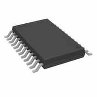
AD7470ARUZ Analog Devices Inc, AD7470ARUZ Datasheet - Page 5

AD7470ARUZ
Manufacturer Part Number
AD7470ARUZ
Description
IC ADC 10BIT PARALLEL 24-TSSOP
Manufacturer
Analog Devices Inc
Datasheet
1.AD7470ARUZ.pdf
(6 pages)
Specifications of AD7470ARUZ
Data Interface
Parallel
Number Of Bits
10
Sampling Rate (per Second)
1.75M
Number Of Converters
1
Power Dissipation (max)
12mW
Voltage Supply Source
Analog and Digital
Operating Temperature
-40°C ~ 85°C
Mounting Type
Surface Mount
Package / Case
24-TSSOP (0.173", 4.40mm Width)
Resolution (bits)
10bit
Input Channel Type
Single Ended
Supply Voltage Range - Analogue
2.7V To 5.25V
Supply Voltage Range - Digital
2.7V To 5.25V
Supply
RoHS Compliant
Sampling Rate
1.75MSPS
Rohs Compliant
Yes
Number Of Elements
1
Resolution
10Bit
Architecture
SAR
Sample Rate
1.75MSPS
Input Polarity
Unipolar
Input Type
Voltage
Rated Input Volt
2.5V
Differential Input
No
Power Supply Requirement
Analog and Digital
Single Supply Voltage (typ)
3/5V
Single Supply Voltage (min)
2.7V
Single Supply Voltage (max)
5.25V
Dual Supply Voltage (typ)
Not RequiredV
Dual Supply Voltage (min)
Not RequiredV
Dual Supply Voltage (max)
Not RequiredV
Power Dissipation
12mW
Differential Linearity Error
±0.9LSB
Integral Nonlinearity Error
±1LSB
Operating Temp Range
-40C to 85C
Operating Temperature Classification
Industrial
Mounting
Surface Mount
Pin Count
24
Package Type
TSSOP
Input Signal Type
Single-Ended
Lead Free Status / RoHS Status
Lead free / RoHS Compliant
Lead Free Status / RoHS Status
Lead free / RoHS Compliant
Available stocks
Company
Part Number
Manufacturer
Quantity
Price
Part Number:
AD7470ARUZ
Manufacturer:
ADI/亚德诺
Quantity:
20 000
TIMING SPECIFICATIONS
Parameter
f
t
t
t
t
t
t
t
t
t
t
t
t
NOTES
1
2
3
4
Specifications subject to change without notice.
REV. B
CLK
CONVERT
WAKEUP
1
2
3
4
5
6
7
8
9
10
Sample tested at 25°C to ensure compliance. All input signals are specified with tr = tf = 5 ns (10% to 90% of V
See Figure 1.
Mark/Space ratio for the CLK inputs is 40/60 to 60/40. First CLK pulse should be 10 ns min from falling edge of CONVST.
Measured with the load circuit of Figure 1 and defined as the time required for the output to cross 0.8 V or 2.0 V.
t
back to remove the effects of charging or discharging the 50 pF capacitor. This means that the time, t
time of the part and is independent of the bus loading.
7
3
3
4
is derived from the measured time taken by the data outputs to change 0.5 V when loaded with the circuit of Figure 1. The measured number is then extrapolated
2
AD7470
10
30
436.42
1
10
10
30
0
0
20
15
8
0
135
100
Limit at T
Figure 1. Load Circuit for Digital Output Timing Specifications
1
(V
MIN
DD
, T
AD7472
10
26
531.66
1
10
10
15
30
35
0
0
20
15
8
0
135
140
100
= 2.7 V to 5.25 V, REF IN = 2.5 V; T
MAX
TO OUTPUT
PIN
50pF
C
L
200 A
200 A
–5–
Unit
kHz min
MHz max
ns min
µs max
ns min
ns max
ns max
ns max
ns max
ns max
ns max
ns min
ns min
ns max
ns max
ns max
ns max
ns min
I
I
OL
OH
A
= T
MIN
1.6V
7
, quoted in the timing characteristics, is the true bus relinquish
to T
Description
t
Wake-Up Time
CONVST Pulse Width
CONVST to BUSY Delay,
V
V
V
V
BUSY to CS Setup Time
CS to RD Setup Time
RD Pulse Width
Data Access Time After Falling Edge of RD
Bus Relinquish Time After Rising Edge of RD
CS to RD Hold Time
Acquisition Time
A and B Versions
Y Version
Quiet Time
MAX
CLK
DD
DD
DD
DD
, unless otherwise noted.)
DD
= 1/f
= 5 V, A and B Versions
= 5 V, Y Version
= 3 V, A and B Versions
= 3 V, Y Version
) and timed from a voltage level of 1.6 V.
CLK IN
AD7470/AD7472


