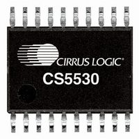
CS5530-ISZ Cirrus Logic Inc, CS5530-ISZ Datasheet - Page 32

CS5530-ISZ
Manufacturer Part Number
CS5530-ISZ
Description
IC ADC 24BIT 1CH W/LNA 20SSOP
Manufacturer
Cirrus Logic Inc
Datasheet
1.CS5530-ISZ.pdf
(36 pages)
Specifications of CS5530-ISZ
Number Of Converters
1
Package / Case
20-SSOP
Number Of Bits
24
Sampling Rate (per Second)
3.84k
Data Interface
Serial
Power Dissipation (max)
45mW
Voltage Supply Source
Analog and Digital, Dual ±
Operating Temperature
-40°C ~ 85°C
Mounting Type
Surface Mount
Number Of Adc Inputs
1
Architecture
Delta-Sigma
Conversion Rate
6.25 SPs to 3840 SPs
Resolution
24 bit
Input Type
Voltage
Interface Type
Serial (3-Wire)
Voltage Reference
2.5 V
Maximum Power Dissipation
500 mW
Maximum Operating Temperature
+ 85 C
Mounting Style
SMD/SMT
Minimum Operating Temperature
- 40 C
Lead Free Status / RoHS Status
Lead free / RoHS Compliant
For Use With
598-1158 - BOARD EVAL FOR CS5530
Lead Free Status / Rohs Status
Lead free / RoHS Compliant
Other names
598-1283-5
Available stocks
Company
Part Number
Manufacturer
Quantity
Price
Company:
Part Number:
CS5530-ISZ
Manufacturer:
CIRRUS
Quantity:
1 529
Part Number:
CS5530-ISZ
Manufacturer:
CIRRUS
Quantity:
20 000
Company:
Part Number:
CS5530-ISZR
Manufacturer:
CIRRUS
Quantity:
1 000
3. PIN DESCRIPTIONS
Clock Generator
OSC1; OSC2 – Master Clock
Control Pins and Serial Data I/O
CS – Chip Select
SDI – Serial Data Input
SDO – Serial Data Output
SCLK – Serial Clock Input
A0 – Logic Output (Analog), A1 – Logic Output (Analog)
32
AMPLIFIER CAPACITOR CONNECT
AMPLIFIER CAPACITOR CONNECT
DIFFERENTIAL ANALOG INPUT
An inverting amplifier inside the chip is connected between these pins and can be used with a
crystal to provide the master clock for the device. Alternatively, an external (CMOS compatible)
clock (powered relative to VD+) can be supplied into the OSC2 pin to provide the master clock
for the device.
When active low, the port will recognize SCLK. When high the SDO pin will output a high
impedance state. CS should be changed when SCLK = 0.
SDI is the input pin of the serial input port. Data will be input at a rate determined by SCLK.
A clock signal on this pin determines the input/output rate of the data for the SDI/SDO pins
respectively. This input is a Schmitt trigger to allow for slow rise time signals. The SCLK pin
will recognize clocks only when CS is low.
The logic states of A1-A0 mimic the A1-A0 bits in the Configuration Register. Logic
Output 0 = VA-, and Logic Output 1 = VA+.
DIFFERENTIAL ANALOG INPUT
SDO is the serial data output. It will output a high impedance state if CS = 1.
NEGATIVE ANALOG POWER
POSITIVE ANALOG POWER
LOGIC OUTPUT (ANALOG)
LOGIC OUTPUT (ANALOG)
MASTER CLOCK
MASTER CLOCK
AIN1+
OSC2
OSC1
AIN1-
VA+
VA-
C1
C2
A0
A1
1
2
3
4
5
6
7
8
9
10
CS5530
20
19
18
17
16
15
14
13
12
11
NC
VREF+
VREF-
DGND
VD+
CS
SDI
SDO
SCLK
NC
VOLTAGE REFERENCE INPUT
VOLTAGE REFERENCE INPUT
DIGITAL GROUND
POSITIVE DIGITAL POWER
CHIP SELECT
SERIAL DATA INPUT
SERIAL DATA OUT
SERIAL CLOCK INPUT
CS5530
DS742F3


