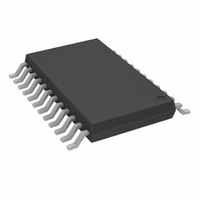
AD7795BRUZ Analog Devices Inc, AD7795BRUZ Datasheet - Page 7

AD7795BRUZ
Manufacturer Part Number
AD7795BRUZ
Description
IC ADC 16BIT 6CH LOW-PWR 24TSSOP
Manufacturer
Analog Devices Inc
Datasheet
1.AD7795BRUZ.pdf
(36 pages)
Specifications of AD7795BRUZ
Data Interface
DSP, MICROWIRE™, QSPI™, Serial, SPI™
Number Of Bits
16
Sampling Rate (per Second)
470
Number Of Converters
1
Power Dissipation (max)
2.5mW
Voltage Supply Source
Analog and Digital
Operating Temperature
-40°C ~ 105°C
Mounting Type
Surface Mount
Package / Case
24-TSSOP (0.173", 4.40mm Width)
Resolution (bits)
16bit
Sampling Rate
470SPS
Input Channel Type
Differential
Supply Voltage Range - Analog
2.7V To 5.25V
Supply Voltage Range - Digital
2.7V To 5.25V
Number Of Elements
1
Resolution
16Bit
Architecture
Delta-Sigma
Sample Rate
0.47KSPS
Input Polarity
Bipolar
Input Type
Voltage
Rated Input Volt
±2.5V
Differential Input
Yes
Power Supply Requirement
Single
Single Supply Voltage (typ)
3.3/5V
Single Supply Voltage (min)
2.7V
Single Supply Voltage (max)
5.25V
Dual Supply Voltage (typ)
Not RequiredV
Dual Supply Voltage (min)
Not RequiredV
Dual Supply Voltage (max)
Not RequiredV
Power Dissipation
2.5mW
Integral Nonlinearity Error
±15ppm of FSR
Operating Temp Range
-40C to 105C
Operating Temperature Classification
Industrial
Mounting
Surface Mount
Pin Count
24
Package Type
TSSOP
Input Signal Type
Differential
Lead Free Status / RoHS Status
Lead free / RoHS Compliant
Lead Free Status / RoHS Status
Lead free / RoHS Compliant, Lead free / RoHS Compliant
Available stocks
Company
Part Number
Manufacturer
Quantity
Price
Company:
Part Number:
AD7795BRUZ
Manufacturer:
ADI
Quantity:
1 000
Part Number:
AD7795BRUZ
Manufacturer:
ADI/亚德诺
Quantity:
20 000
Company:
Part Number:
AD7795BRUZ-REEL
Manufacturer:
SHINDENGEN
Quantity:
2 400
Company:
Part Number:
AD7795BRUZ-REEL
Manufacturer:
ADI
Quantity:
1 000
Part Number:
AD7795BRUZ-REEL
Manufacturer:
ADI/亚德诺
Quantity:
20 000
Parameter
LOGIC OUTPUT (INCLUDING CLK)
SYSTEM CALIBRATION
POWER REQUIREMENTS
1
2
3
4
5
6
7
Temperature range: B Grade: −40°C to +105°C, C Grade: −40°C to +125°C. At the 19.6 Hz and 39.2 Hz update rates, the INL, power supply rejection (PSR), common-
mode rejection (CMR), and normal mode rejection (NMR) do not meet the data sheet specification if the voltage on the AIN(+) or AIN(−) pins exceeds AV
typically. In addition, the offset error and offset error drift degrade at these update rates when chopping is disabled. When this voltage is exceeded, the INL, for
example, is reduced to 18 ppm of FS typically while the PSR is reduced to 69 dB typically. Therefore, for guaranteed performance at these update rates, the absolute
voltage on the analog input pins needs to be below AVDD − 1.6 V.
Specification is not production tested but is supported by characterization data at initial product release.
Following a calibration, this error is in the order of the noise for the programmed gain and update rate selected.
Recalibration at any temperature removes these errors.
Full-scale error applies to both positive and negative full-scale, and applies at the factory calibration conditions (AV
FS[3:0] are the four bits used in the mode register to select the output word rate.
Digital inputs equal to DV
V
V
V
V
Floating-State Leakage Current
Floating-State Output Capacitance
Data Output Coding
Full-Scale Calibration Limit
Zero-Scale Calibration Limit
Input Span
Power Supply Voltage
Power Supply Currents
OH
OL
OH
OL
AV
DV
I
I
, Output Low Voltage
, Output Low Voltage
DD
DD
, Output High Voltage
, Output High Voltage
DD
DD
Current
(Power-Down Mode)
to GND
to GND
1
2
DD
7
or GND with excitation currents and bias voltage generator disabled.
2
2
2
2
AD7794/AD7795
DV
0.4
4
0.4
±10
10
Offset binary
1.05 × FS
−1.05 × FS
0.8 × FS
2.1 × FS
2.7/5.25
2.7/5.25
140
185
400
500
1
2
DD
− 0.6
Rev. D | Page 7 of 36
Unit
V min
V max
V min
V max
μA max
pF typ
V max
V min
V min
V max
V min/max
V min/max
μA max
μA max
μA max
μA max
μA max
μA max
Test Conditions/Comments
DV
DV
DV
DV
110 μA typ @ AV
unbuffered mode, external reference
130 μA typ @ AV
buffered mode, gain = 1 or 2, external reference
300 μA typ @ AV
gain = 4 to 128, external reference
400 μA typ @ AV
gain = 4 to 128, internal reference
AD7794B, AD7795B
AD7794C
DD
DD
DD
DD
= 3 V, I
= 3 V, I
= 5 V, I
= 5 V, I
DD
SOURCE
SINK
SOURCE
SINK
= 4 V, gain = 1, T
= 100 μA
= 1.6 mA (DOUT/RDY), 800 μA (CLK)
DD
DD
DD
DD
= 100 μA
= 200 μA
= 3 V, 125 μA typ @ AV
= 3 V, 165 μA typ @ AV
= 3 V, 350 μA typ @ AV
= 3 V, 450 μA typ @ AV
A
= 25°C).
AD7794/AD7795
DD
DD
DD
DD
DD
= 5 V,
= 5 V,
= 5 V,
= 5 V,
– 1.6 V


