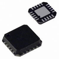
AD7699BCPZ Analog Devices Inc, AD7699BCPZ Datasheet - Page 19

AD7699BCPZ
Manufacturer Part Number
AD7699BCPZ
Description
IC ADC 8CH 16BIT 500KSPS 20LFCSP
Manufacturer
Analog Devices Inc
Datasheet
1.AD7699BCPZ.pdf
(28 pages)
Specifications of AD7699BCPZ
Data Interface
DSP, MICROWIRE™, QSPI™, Serial, SPI™
Number Of Bits
16
Sampling Rate (per Second)
500k
Number Of Converters
1
Power Dissipation (max)
32mW
Voltage Supply Source
Single Supply
Operating Temperature
-40°C ~ 85°C
Mounting Type
Surface Mount
Package / Case
20-VFQFN, CSP Exposed Pad
Resolution (bits)
16bit
Sampling Rate
500kSPS
Input Channel Type
Pseudo Differential, Single Ended
Supply Voltage Range - Analog
4.5V To 5.5V
Lead Free Status / RoHS Status
Lead free / RoHS Compliant
Available stocks
Company
Part Number
Manufacturer
Quantity
Price
Company:
Part Number:
AD7699BCPZ
Manufacturer:
ADI
Quantity:
490
Part Number:
AD7699BCPZ
Manufacturer:
ADI/亚德诺
Quantity:
20 000
reference, or a low impedance buffer such as the
AD8605.
The placement of the reference decoupling capacitor is also
important to the performance of the AD7699, as explained in the
Layout section. Mount the decoupling capacitor on the same side
as the ADC at the REF pin with a thick PCB trace. The GND
should also connect to the reference decoupling capacitor with
the shortest distance and to the analog ground plane with
several vias.
If desired, smaller reference decoupling capacitor values down
to 2.2 µF can be used with a minimal impact on performance,
especially on DNL.
Regardless, there is no need for an additional lower value
ceramic decoupling capacitor (for example, 100 nF) between the
REF and GND pins.
For applications that use multiple AD7699s or other PulSAR
devices, it is more effective to use the internal reference buffer
to buffer the external reference voltage, thus reducing SAR
conversion crosstalk.
The voltage reference temperature coefficient (TC) directly
impacts full scale; therefore, in applications where full-scale
accuracy matters, care must be taken with the TC. For instance,
a ±15 ppm/°C TC of the reference changes full scale by ±1 LSB/°C.
POWER SUPPLY
The AD7699 uses two power supply pins: an analog and digital
core supply (VDD) and a digital input/output interface supply
(VIO). VIO allows direct interface with any logic between 1.8 V
and VDD. To reduce the supplies needed, the VIO and VDD
pins can be tied together. The AD7699 is independent of power
supply sequencing between VIO and VDD. The only restriction
is that CNV must be low when powering up the AD7699.
Additionally, it is very insensitive to power supply variations
over a wide frequency range, as shown in Figure 32.
75
70
65
60
55
50
45
40
35
30
1
Figure 32. PSRR vs. Frequency
10
FREQUENCY (kHz)
100
1k
AD8031
10k
or the
Rev. 0 | Page 19 of 28
The AD7699 powers down automatically at the end of each
conversion phase; therefore, the operating currents and power
scale linearly with the sampling rate. This makes the part ideal
for low sampling rates (even of a few hertz) and low battery-
powered applications.
SUPPLYING THE ADC FROM THE REFERENCE
For simplified applications, the AD7699, with its low operating
current, can be supplied directly using the reference circuit, as
shown in Figure 34. The reference line can be driven by
•
•
•
1
5V
OPTIONAL REFERENCE BUFFER AND FILTER.
The system power supply directly
A reference voltage with enough current output capability,
such as the
A reference buffer, such as the AD8605, which can also
filter the system power supply, as shown in Figure 34
10,000
10kΩ
0.010
0.001
1000
1µF
100
0.1
10
1
10
Figure 33. Operating Currents vs. Sampling Rate
VDD = 5V, INTERNAL REF
Figure 34. Example of an Application Circuit
5V
ADR43x/ADR44x
AD8605
VDD = 5V, EXTERNAL REF
100
1
SAMPLING RATE (sps)
10µF
1k
5V
REF
10k
10Ω
1µF
AD7699
VIO
VDD
0.1µF
100k
AD7699
VIO
0.1µF
1M


