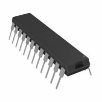
AD7730BNZ Analog Devices Inc, AD7730BNZ Datasheet - Page 18

AD7730BNZ
Manufacturer Part Number
AD7730BNZ
Description
IC ADC TRANSDUCER BRIDGE 24-DIP
Manufacturer
Analog Devices Inc
Datasheet
1.AD7730LBRUZ.pdf
(52 pages)
Specifications of AD7730BNZ
Data Interface
DSP, Serial, SPI™
Number Of Bits
24
Sampling Rate (per Second)
1.2k
Number Of Converters
1
Power Dissipation (max)
125mW
Voltage Supply Source
Analog and Digital
Operating Temperature
-40°C ~ 85°C
Mounting Type
Through Hole
Package / Case
24-DIP (0.300", 7.62mm)
Resolution (bits)
24bit
Sampling Rate
1.2kSPS
Input Channel Type
Differential, Single Ended
Supply Voltage Range - Analog
4.75V To 5.25V
Lead Free Status / RoHS Status
Lead free / RoHS Compliant
For Use With
EVAL-AD7730LEBZ - BOARD EVALUATION FOR AD7730EVAL-AD7730EBZ - BOARD EVAL FOR AD7730
Lead Free Status / RoHS Status
Lead free / RoHS Compliant, Lead free / RoHS Compliant
AD7730/AD7730L
Bit
Location
MR2
MR1–MR0
Filter Register (RS2-RS0 = 0, 1, 1); Power-On/Reset Status: 200010 Hex
The Filter Register is a 24-bit register from which data can be read or to which data can be written. This register determines the
amount of averaging performed by the filter and the mode of operation of the filter. It also sets the chopping mode and the delay
associated with chopping the inputs. Table XIV outlines the bit designations for the Filter Register. FR0 through FR23 indicate the
bit location, FR denoting the bits are in the Filter Register. FR23 denotes the first bit of the data stream. The number in brackets
indicates the power-on/reset default status of that bit. Figure 5 shows a flowchart for reading from the registers on the AD7730 and
Figure 6 shows a flowchart for writing to the registers on the part.
Bit
Location
FR23–FR12
ZERO (0)
SF11 (0)
SF3 (0)
Bit
Mnemonic
BO
CH1–CH0
Bit
Mnemonic
SF11–SF0
FR23
FR15
FR7
ZERO (0)
SF10 (0)
SF2 (0)
FR22
FR14
FR6
Description
Burnout Current Bit. A 1 in this bit activates the burnout currents. When active, the burnout currents
connect to the selected analog input pair, one source current to the AIN(+) input and one sink current to
the AIN(–) input. A 0 in this bit turns off the on-chip burnout currents.
Channel Selection Bits. These bits select the analog input channel to be converted or calibrated as
outlined in Table XIII. With CH1 at 1 and CH0 at 0, the part looks at the AIN1(–) input internally
shorted to itself. This can be used as a test method to evaluate the noise performance of the part with
no external noise sources. In this mode, the AIN1(–) input should be connected to an external voltage
within the allowable common-mode range of the part. The Offset and Gain Calibration Registers on
the part are paired. There are three pairs of calibration registers labelled Register Pair 0 through Regis-
ter Pair 2. These are assigned to the input channel pairs as outlined in Table XIII.
Description
Sinc
programmed to SF11 through SF0 set the amount of averaging the sinc
the number programmed to these 12 bits affects the –3 dB frequency and output update rate from the
part (see Filter Architecture section). The allowable range for SF words depends on whether the part
is operated with CHOP on or off and SKIP on or off. Table XV outlines the SF ranges for different
setups. All output update rates will be one-half those quoted in Table XV for the AD7730L operating
with a 2.4576 MHz clock.
CH1
0
0
1
1
3
Filter Selection Bits. The AD7730 contains two filters: a sinc
CH0
0
1
0
1
SF1 (0)
SF9 (1)
AC (0)
FR21
FR13
FR5
Table XIV. Filter Register
CHP (1)
Positive Input
AIN1(+)
AIN2(+)
AIN1(–)
AIN1(–)
SF8 (0)
SF0 (0)
FR20
FR12
FR4
Table XIII. Channel Selection
Input Channel Pair
–18–
ZERO (0)
DL3 (0)
SF7 (0)
FR19
FR11
FR3
Negative Input
AIN1(–)
AIN2(–)
AIN1(–)
AIN2(–)
ZERO (0)
DL2 (0)
SF6 (0)
FR18
FR10
FR2
SKIP (0)
DL1 (0)
3
SF5 (0)
FR17
filter and an FIR filter. The 12 bits
FR9
FR1
Calibration Register Pair
Register Pair 0
Register Pair 1
Register Pair 0
Register Pair 2
3
filter performs. As a result,
FAST (0)
DL0 (0)
SF4 (0)
FR16
FR8
FR0
REV. A


