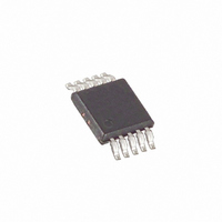
MAX1108EUB+ Maxim Integrated Products, MAX1108EUB+ Datasheet - Page 11

MAX1108EUB+
Manufacturer Part Number
MAX1108EUB+
Description
IC ADC 8BIT LP 10-UMAX
Manufacturer
Maxim Integrated Products
Datasheet
1.MAX1109EUB.pdf
(20 pages)
Specifications of MAX1108EUB+
Number Of Bits
8
Sampling Rate (per Second)
50k
Data Interface
MICROWIRE™, QSPI™, Serial, SPI™
Number Of Converters
1
Power Dissipation (max)
444mW
Voltage Supply Source
Single Supply
Operating Temperature
-40°C ~ 85°C
Mounting Type
Surface Mount
Package / Case
10-MSOP, Micro10™, 10-uMAX, 10-uSOP
Number Of Adc Inputs
2
Architecture
SAR
Conversion Rate
50 KSPs
Resolution
8 bit
Interface Type
Serial
Voltage Reference
Internal 2.048 V or External
Supply Voltage (max)
3.3 V
Mounting Style
SMD/SMT
Lead Free Status / RoHS Status
Lead free / RoHS Compliant
holding capacitor C
acquisition the T/H switch opens and C
nected to COM, retaining charge on C
ple of the signal at CH0, and the difference between
CH0 and COM is the converted signal. Once conver-
sion is complete, the T/H returns immediately to its
tracking mode. This procedure holds for the different
combinations summarized in Table 2.
The time available for the T/H to acquire an input signal
(t
at the maximum clock frequency of 2MHz. The acquisi-
tion time is also the minimum time needed for the signal
to be acquired. It is calculated by:
where R
the input signal, and t
Note that source impedances below 2.7k
significantly affect the AC performance of the ADC at
the maximum clock speed. If the input-source imped-
ance is higher than 3k , the clock speed must be
reduced accordingly.
The MAX1108/MAX1109 input configuration is pseudo-
differential to the extent that only the signal at the sam-
pled input (SI) is stored in the holding capacitor
(C
within ±0.5LSB (±0.1LSB for best results) in relation to
GND during a conversion. Sampled input and refer-
ence input configuration is determined by bit6–bit4
(SEL2–SEL0) of the control byte (Table 2).
If a varying signal is applied at the selected reference
input, its amplitude and frequency need to be limited.
The following equations determine the relationship
between the maximum signal amplitude and its fre-
quency to maintain ±0.5LSB accuracy:
Assuming a sinusoidal signal at the reference input
the maximum voltage variation is determined by:
a 60Hz signal at RI with an amplitude of 1.2V will gener-
ate a ±0.5LSB of error. This is with a 35µs conversion
time (maximum t
a reference voltage of +4.096V. When a DC reference
voltage is used at RI, connect a 0.1µF capacitor to
GND to minimize noise at the input.
ACQ
HOLD
max
) is determined by the clock frequency, and is 1µs
dv
). The reference input (RI) must remain stable
dt
IN
RI
= 6.5k , R
2 f v
t
ACQ
CONV
v
______________________________________________________________________________________
RI
RI
HOLD
= 6(R
in internal conversion mode) and
S
ACQ
V sin(2 ft)
= the source impedance of
RI
S
t
1 LSB
through R
CONV
+ R
Pseudo-Differential Input
is never less than 1µs.
IN
)18pF
IN
2 t
HOLD
8
. At the end of
V
REF
CONV
HOLD
as a sam-
2-Channel, Serial 8-Bit ADCs
is con-
do not
Single-Supply, Low-Power,
The input configuration selection also determines
unipolar or bipolar conversion mode. The common-
mode input range of CH0, CH1, and COM is 0 to +V
In unipolar mode, full scale is achieved when (SI - RI) =
V
- RI) = V
than RI; in bipolar mode, SI can span above and below
RI provided that it is within the common-mode range.
The comparator negative input is connected to the auto-
zero rail. Since the device requires only a single supply,
the ZERO node at the input of the comparator equals
V
0V difference at the comparator inputs within the limits
of 8-bit resolution. This action is equivalent to transfer-
ring a charge of 18pF(V
binary-weighted capacitive DAC which, in turn, forms a
digital representation of the analog-input signal.
Internal protection diodes that clamp the analog input
to V
CH1, and COM) to swing from (AGND - 0.3V) to (V
0.3V) without damage. However, for accurate conver-
sions, the inputs must not exceed (V
less than (GND - 50mV).
If the analog input voltage on an “off” channel
exceeds 50mV beyond the supplies, the current
should be limited to 2mA to maintain conversion
accuracy on the “on” channel.
The MAX1108/MAX1109 input range is from 0 to V
unipolar or bipolar conversion is available. In unipolar
mode, the output code is invalid (code zero) when a
negative input voltage (or a negative differential input
voltage) is applied. The reference input-voltage range
at REF is from 1V to (V
The ADC’s input tracking circuitry has a 1.5MHz small-
signal bandwidth, so it is possible to digitize high-
speed transient events and measure periodic signals
with bandwidths exceeding the ADC’s sampling rate by
using undersampling techniques. To avoid high-fre-
quency signals being aliased into the frequency band
of interest, anti-alias filtering is recommended.
The MAX1108/MAX1109 have a 4-wire serial interface.
The CS, DIN, and SCLK inputs are used to control the
device, while the three-state DOUT pin is used to
access the result of conversion.
REF
DD
/2. The capacitive DAC restores node ZERO to have
DD
; in bipolar mode, full scale is achieved when (SI
and AGND allow the channel input pins (CH0,
REF
/ 2. In unipolar mode, SI must be higher
DD
IN+
+ 50mV.)
- V
IN-
Conversion Process
Input Voltage Range
) from C
Serial Interface
DD
Input Bandwidth
+ 50mV) or be
HOLD
to the
DD
DD
DD
11
+
.
;


