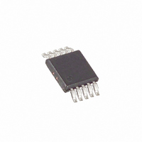
MAX1108EUB+ Maxim Integrated Products, MAX1108EUB+ Datasheet - Page 14

MAX1108EUB+
Manufacturer Part Number
MAX1108EUB+
Description
IC ADC 8BIT LP 10-UMAX
Manufacturer
Maxim Integrated Products
Datasheet
1.MAX1109EUB.pdf
(20 pages)
Specifications of MAX1108EUB+
Number Of Bits
8
Sampling Rate (per Second)
50k
Data Interface
MICROWIRE™, QSPI™, Serial, SPI™
Number Of Converters
1
Power Dissipation (max)
444mW
Voltage Supply Source
Single Supply
Operating Temperature
-40°C ~ 85°C
Mounting Type
Surface Mount
Package / Case
10-MSOP, Micro10™, 10-uMAX, 10-uSOP
Number Of Adc Inputs
2
Architecture
SAR
Conversion Rate
50 KSPs
Resolution
8 bit
Interface Type
Serial
Voltage Reference
Internal 2.048 V or External
Supply Voltage (max)
3.3 V
Mounting Style
SMD/SMT
Lead Free Status / RoHS Status
Lead free / RoHS Compliant
Single-Supply, Low-Power,
2-Channel, Serial 8-Bit ADCs
initiated. The MSB successive-approximation bit deci-
sion is made on the rising edge of the seventh SCLK.
On the falling edge of the eighth SCLK, the MSB is
clocked out on the DOUT pin; on each of the next
seven SCLK falling edges, the remaining bits of conver-
sion are clocked out. Zeros are clocked out on DOUT
after the LSB has been clocked out, until CS is dis-
abled. Then DOUT becomes high impedance and the
part is ready for another conversion (Figure 6).
The conversion must complete in 1ms, or droop on the
sample-and-hold capacitors may degrade conversion
results. Use internal clock mode if the serial-clock fre-
quency is less than 50kHz, or if serial-clock interruptions
could cause the conversion interval to exceed 1ms.
Figure 6. Single Conversion Timing, External Clock Mode
Figure 7. Detailed Serial-Interface Timing
14
DOUT
A/D STATE
SCLK
DIN
CS
______________________________________________________________________________________
SCLK
DOUT
DIN
CS
START
MSB
t
1
CSH
SEL2
IDLE
SEL1
t
t
DV
CSS
t
DS
SEL0
t
DH
4
I/ECLK I/EREF
t
ACQ
t
CL
SHDN
REF
SHDN
LSB
t
8
CH
MSB
D7
D6
Internal clock mode frees the µP from the burden of
running the SAR conversion clock. This allows the con-
version results to be read back at the processor’s con-
venience, at any clock rate up to 2MHz.
An internal register stores data when the conversion is
in progress. On the falling edge of the fourth SCLK,
track mode is enabled, and on the falling edge of the
eighth SCLK, acquisition is complete and internal con-
version is initiated. The internal 400kHz clock com-
pletes the conversion in 20µs typically (35µs max), at
which time the MSB of the conversion is present at the
DOUT pin. The falling edge of SCLK clocks the remain-
ing data out of this register at any time after the conver-
sion is complete (Figure 8).
D5
t
CONV
D4
12
D3
t
DO
D2
D1
LSB
D0
16
t
CSH
IDLE
t
TR
Internal Clock
20


