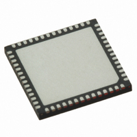
MAX11044ETN+ Maxim Integrated Products, MAX11044ETN+ Datasheet - Page 16

MAX11044ETN+
Manufacturer Part Number
MAX11044ETN+
Description
ADC 16BIT SAMPLING 4CH 56-TQFN
Manufacturer
Maxim Integrated Products
Datasheet
1.MAX11044ETN.pdf
(27 pages)
Specifications of MAX11044ETN+
Number Of Bits
16
Sampling Rate (per Second)
250k
Data Interface
Parallel
Number Of Converters
4
Power Dissipation (max)
2.22W
Voltage Supply Source
Analog and Digital
Operating Temperature
-40°C ~ 85°C
Mounting Type
Surface Mount
Package / Case
56-WQFN Exposed Pad, 56-HWQFN
Number Of Adc Inputs
4
Architecture
SAR
Conversion Rate
250 KSPs
Resolution
16 bit
Input Type
Voltage
Interface Type
Parallel
Snr
92.3 dB
Voltage Reference
Internal 4.096 V
Supply Voltage (max)
5.25 V
Supply Voltage (min)
2.7 V, 4.75 V
Maximum Power Dissipation
2222 mW
Maximum Operating Temperature
+ 85 C
Mounting Style
SMD/SMT
Input Voltage
5 V
Minimum Operating Temperature
- 40 C
Lead Free Status / RoHS Status
Lead free / RoHS Compliant
4-/6-/8-Channel, 16-/14-Bit,
Simultaneous-Sampling ADCs
is driven by an internal bandgap reference circuit (V
FIO
bypass with 0.1µF capacitor to ground when using the
internal reference.
To preserve phase information across all channels,
each input includes a dedicated T/H circuitry. The input
tracking circuitry provides a 4MHz small-signal band-
width, enabling the device to digitize high-speed tran-
sient events and measure periodic signals with
bandwidths exceeding the ADC’s sampling rate by
using undersampling techniques. Use anti-alias filtering
to avoid high-frequency signals being aliased into the
frequency band of interest.
The full-scale analog input voltage is a product of the ref-
erence voltage. For the MAX11044/MAX11045/
MAX11046 and MAX11054/MAX11055/MAX11056, the
full-scale input is bipolar in the range of:
Figure 1. Required Setup for Clamp Circuit
= 4.096V). Drive REFIO with an external reference or
SIGNAL
±(
INPUT
16
V
REFIO
SOURCE
______________________________________________________________________
R
S
x
Input Range and Protection
VOLTAGE
4 096
.
PIN
5
AGNDS
AGND
REFIO
AVDD
CH7
CH0
)
Track and Hold (T/H)
†
**MAX11044/MAX11045/MAX11046
*CONNECTED INTERNALLY ON THE TQFN PARTS TO RDC
†
MAX11046/MAX11056
Analog Inputs
MAX11044/MAX11045/MAX11046/
MAX11054/MAX11055/MAX11056
REFERENCE
BANDGAP
CLAMP
CLAMP
10kΩ
S/H
S/H
RE-
EXT REF
INT REF
16-/14-BIT ADC
16-/14-BIT ADC
When in external reference mode, drive V
3.0V to 4.25V source, resulting in an input range of
±3.662V to ±5.188V, respectively.
All analog inputs are fault-protected to up to ±20mA.
The MAX11044/MAX11045/MAX11046 and MAX11054/
MAX11055/MAX11056 include an input clamping circuit
that activates when the input voltage at the analog input
is above (V
The clamp circuit remains high impedance while the
input signal is within the range of ±V
tle or almost no current. However, when the input signal
exceeds ±V
shunt current to/from the AVDD supply. Consequently,
to obtain the highest accuracy, ensure that the input
voltage does not exceed ±(V
To make use of the input clamps (see Figure 1), con-
nect a resistor (R
voltage source to limit the voltage at the analog input so
that the fault current into the MAX11044/MAX11045/
MAX11046 and MAX11054/MAX11055/MAX11056 does
not exceed ±20mA. Note that the voltage at the analog
input pin limits to approximately 7V during a fault condi-
tion so the following equation can be used to calculate
the value of R
REF
BUF
AVDD
AVDD
S
:
CONFIGURATION
REGISTERS
INTERFACE
+ 300mV) or below –(V
CONTROL
S
, the clamps begin to turn on and
AND
) between the analog input and the
AVDD
RDC
RDC_SENSE*
DB15**
DB4
DB3/CR3
DB0/CR0
WR
RD
CS
CONVST
SHDN
EOC
DGND
DVDD
+ 0.3V).
AVDD
AVDD
and draws lit-
REFIO
+ 300mV).
with a


