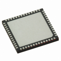
MAX11044ETN+ Maxim Integrated Products, MAX11044ETN+ Datasheet - Page 2

MAX11044ETN+
Manufacturer Part Number
MAX11044ETN+
Description
ADC 16BIT SAMPLING 4CH 56-TQFN
Manufacturer
Maxim Integrated Products
Datasheet
1.MAX11044ETN.pdf
(27 pages)
Specifications of MAX11044ETN+
Number Of Bits
16
Sampling Rate (per Second)
250k
Data Interface
Parallel
Number Of Converters
4
Power Dissipation (max)
2.22W
Voltage Supply Source
Analog and Digital
Operating Temperature
-40°C ~ 85°C
Mounting Type
Surface Mount
Package / Case
56-WQFN Exposed Pad, 56-HWQFN
Number Of Adc Inputs
4
Architecture
SAR
Conversion Rate
250 KSPs
Resolution
16 bit
Input Type
Voltage
Interface Type
Parallel
Snr
92.3 dB
Voltage Reference
Internal 4.096 V
Supply Voltage (max)
5.25 V
Supply Voltage (min)
2.7 V, 4.75 V
Maximum Power Dissipation
2222 mW
Maximum Operating Temperature
+ 85 C
Mounting Style
SMD/SMT
Input Voltage
5 V
Minimum Operating Temperature
- 40 C
Lead Free Status / RoHS Status
Lead free / RoHS Compliant
4-/6-/8-Channel, 16-/14-Bit,
Simultaneous-Sampling ADCs
ABSOLUTE MAXIMUM RATINGS
AVDD to AGND ........................................................-0.3V to +6V
DVDD to AGND and DGND .....................................-0.3V to +6V
DGND to AGND.....................................................-0.3V to +0.3V
AGNDS to AGND...................................................-0.3V to +0.3V
CH0–CH7 to AGND ...............................................-7.5V to +7.5V
REFIO, RDC to AGND ..................................-0.3V to the lower of
EOC, WR, RD, CS, CONVST to AGND.........-0.3V to the lower of
DB0–DB15 to AGND ....................................-0.3V to the lower of
ELECTRICAL CHARACTERISTICS
(V
33µF, C
noted, f
Stresses beyond those listed under “Absolute Maximum Ratings” may cause permanent damage to the device. These are stress ratings only, and functional
operation of the device at these or any other conditions beyond those indicated in the operational sections of the specifications is not implied. Exposure to
absolute maximum rating conditions for extended periods may affect device reliability.
2
STATIC PERFORMANCE (Note 1)
Resolution
Integral Nonlinearity
Differential Nonlinearity
No Missing Codes
Offset Error
Channel Offset Matching
Offset Temperature Coefficient
Gain Error
Positive Full-Scale Error
Negative Full-Scale Error
Positive Full-Scale Error Matching
Negative Full-Scale Error Matching
Channel Gain-Error Matching
Gain Temperature Coefficient
DYNAMIC PERFORMANCE
Signal-to-Noise Ratio
Signal-to-Noise and Distortion
Ratio
AVDD
_______________________________________________________________________________________
SAMPLE
REFIO
= +4.75V to +5.25V, V
PARAMETER
= 0.1µF, C
= 250ksps. T
AVDD
A
= -40°C to +85°C, unless otherwise noted. Typical values are at T
DVDD
= 4 x 0.1µF || 10µF, C
= +2.70V to +5.25V, V
(V
(V
(V
SYMBOL
DVDD
DVDD
AVDD
SINAD
DNL
SNR
INL
N
+ 0.3V) and +6V
+ 0.3V) and +6V
+ 0.3V) and +6V
MAX11044/MAX11045/MAX11046
MAX11054/MAX11055/MAX11056
MAX11044/MAX11045/MAX11046
MAX11054/MAX11055/MAX11056
MAX11044/MAX11045/MAX11046
MAX11054/MAX11055/MAX11056
MAX11044/MAX11045/MAX11046
MAX11054/MAX11055/MAX11056
Between all channels
f
full-scale input M AX 11054/M AX 11055/
f
full-scale input M AX 11054/M AX 11055/
DVDD
IN
IN
= 10kHz,
= 10kHz,
= 3 x 0.1µF || 10µF; all digital inputs at DVDD or DGND, unless otherwise
AGNDS
CONDITIONS
= V
M AX 11044/M AX 11045/
MAX11046
MAX11056
M AX 11044/M AX 11045/
MAX11046
MAX11056
Maximum Current into Any Pin Except AVDD, DVDD, AGND,
Continuous Power Dissipation
Operating Temperature Range ...........................-40°C to +85°C
Junction Temperature ......................................................+150°C
Storage Temperature Range .............................-65°C to +150°C
Lead Temperature (soldering, 10s) .................................+300°C
Soldering Temperature (reflow) .......................................+260°C
AGND
DGND ...........................................................................±50mA
56-Pin TQFN (derate 47.6mW/°C above +70°C) ....3809.5mW
64-Pin TQFP (derate 43.5mW/°C above +70°C)........3478mW
= V
DGND
= 0V, V
REFIO
84.5
90.5
84.5
MIN
> -2
> -1
-0.8
-0.6
A
16
14
16
14
91
= +25°C.)
= internal reference, C
±0.001
±0.001
±0.13
±0.15
TYP
±0.4
±0.4
±0.8
±0.5
92.3
85.2
85.2
92
±0.015
±0.015
< +1.2
±0.015
±0.015
±0.015
±0.01
±0.01
±0.01
MAX
< +2
+0.8
+0.6
RDC
ppm/°C
UNITS
%FSR
%FSR
%FSR
%FSR
%FSR
%FSR
%FSR
%FSR
µV/°C
LSB
LSB
Bits
Bits
dB
dB
= 4 x


