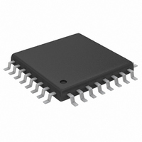
MAX1446EHJ+ Maxim Integrated Products, MAX1446EHJ+ Datasheet - Page 14

MAX1446EHJ+
Manufacturer Part Number
MAX1446EHJ+
Description
IC ADC 10BIT 60MSPS 32-TQFP
Manufacturer
Maxim Integrated Products
Datasheet
1.MAX1446EHJ.pdf
(20 pages)
Specifications of MAX1446EHJ+
Number Of Bits
10
Sampling Rate (per Second)
60M
Data Interface
Parallel
Number Of Converters
1
Voltage Supply Source
Single Supply
Operating Temperature
-40°C ~ 85°C
Mounting Type
Surface Mount
Package / Case
32-TQFP, 32-VQFP
Conversion Rate
60 MSPs
Resolution
10 bit
Snr
59.5 dB
Voltage Reference
2.048 V
Supply Voltage (max)
3.6 V
Supply Voltage (min)
2.7 V
Maximum Power Dissipation
1495.3 mW
Maximum Operating Temperature
+ 85 C
Mounting Style
SMD/SMT
Input Voltage
3 V
Minimum Operating Temperature
- 40 C
Lead Free Status / RoHS Status
Lead free / RoHS Compliant
samples at the falling edge of the input clock. Output
data is valid on the rising edge of the input clock. The
output data has an internal latency of 5.5 clock cycles.
Figure 6 also shows the relationship between the input
clock parameters and the valid output data.
Figure 7 shows a typical application circuit containing a
single-ended to differential converter. The internal refer-
ence provides a V
purposes. The input is buffered and then split to a volt-
age follower and inverter. A lowpass filter follows the op
amps to suppress some of the wideband noise associ-
ated with high-speed op amps. The user may select the
R
to suit a particular application. For the application in
Figure 7, an R
tive load to prevent ringing and oscillation. The 22pF
C
An RF transformer (Figure 8) provides an excellent
solution for converting a single-ended source signal to
a fully differential signal, required by the MAX1446 for
optimum performance. Connecting the transformer’s
center tap to COM provides a V
the input. Although a 1:1 transformer is shown, a step-
up transformer may be selected to reduce the drive
requirements. A reduced signal swing from the input
10-Bit, 60Msps, 3.0V, Low-Power
ADC with Internal Reference
Figure 6. System and Output Timing Diagram
14
ISO
IN
ANALOG INPUT
CLOCK INPUT
DATA OUTPUT
capacitor acts as a small bypassing capacitor.
______________________________________________________________________________________
and C
IN
values to optimize the filter performance
ISO
Applications Information
DD
of 50Ω is placed before the capaci-
Using Transformer Coupling
/2 output voltage for level shifting
t
DO
N - 6
N
DD
/2 DC level shift to
N - 5
N + 1
N - 4
N + 2
5.5 CLOCK-CYCLE LATENCY
driver, such as an op amp, may also improve the over-
all distortion.
In general, the MAX1446 provides better SFDR and
THD with fully differential input signals than single-
ended drive, especially for very high input frequencies.
In differential input mode, even-order harmonics are
lower since both inputs (IN+, IN-) are balanced, and
each of the inputs only requires half the signal swing
compared to single-ended mode.
Figure 9 shows an AC-coupled, single-ended applica-
tion. The MAX4108 op amp provides high speed, high
bandwidth, low noise, and low distortion to maintain the
integrity of the input signal.
Multiple-converter systems based on the MAX1446 are
well suited for use with a common reference voltage.
The REFIN pin of those converters can be connected
directly to an external reference source. A precision
bandgap reference like the MAX6062 generates an
external DC level of 2.048V (Figure 10), and exhibits a
noise voltage density of 150n√Hz. Its output passes
through a 1-pole lowpass filter (with 10Hz cutoff fre-
quency) to the MAX4250, which buffers the reference
before its output is applied to a second 10Hz lowpass
N - 3
N + 3
Buffered External Reference Drives
N - 2
N + 4
N - 1
Single-Ended AC-Coupled
N + 5
N
N + 6
Multiple ADCs
Input Signal
N + 1


