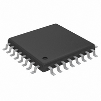
MAX1446EHJ+ Maxim Integrated Products, MAX1446EHJ+ Datasheet - Page 5

MAX1446EHJ+
Manufacturer Part Number
MAX1446EHJ+
Description
IC ADC 10BIT 60MSPS 32-TQFP
Manufacturer
Maxim Integrated Products
Datasheet
1.MAX1446EHJ.pdf
(20 pages)
Specifications of MAX1446EHJ+
Number Of Bits
10
Sampling Rate (per Second)
60M
Data Interface
Parallel
Number Of Converters
1
Voltage Supply Source
Single Supply
Operating Temperature
-40°C ~ 85°C
Mounting Type
Surface Mount
Package / Case
32-TQFP, 32-VQFP
Conversion Rate
60 MSPs
Resolution
10 bit
Snr
59.5 dB
Voltage Reference
2.048 V
Supply Voltage (max)
3.6 V
Supply Voltage (min)
2.7 V
Maximum Power Dissipation
1495.3 mW
Maximum Operating Temperature
+ 85 C
Mounting Style
SMD/SMT
Input Voltage
3 V
Minimum Operating Temperature
- 40 C
Lead Free Status / RoHS Status
Lead free / RoHS Compliant
ELECTRICAL CHARACTERISTICS (continued)
(V
to REFIN through a 10kΩ resistor, V
(50% duty cycle), T
and characterization. Typical values are at T
Note 1: SNR, SINAD, THD, SFDR, and HD3 are based on an analog input voltage of -0.5dBFS referenced to a 1.024V full-scale
Note 2: Intermodulation distortion is the total power of the intermodulation products relative to the individual carrier. This number is
Note 3: Digital outputs settle to V
Note 4: Wake-up time is defined as the time from complete reference power-down until the ADC performs within 0.3 ENOB of the
Note 5: Dynamic characteristics guaranteed at f
Note 6: Guaranteed by design and engineering characterization.
POWER REQUIREMENTS
Analog Supply Voltage
Output Supply Voltage
Analog Supply Current
Output Supply Current
Power-Supply Rejection
TIMING CHARACTERISTICS
CLK Rise to Output Data Valid
OE Fall to Output Enable
OE Rise to Output Disable
Clock Duty Cycle
Wake-Up Time
DD
= 3.0V, OV
input voltage range.
6dB better, if referenced to the two-tone envelope.
final performance for f
2.3µF.
PARAMETER
DD
A
= 2.7V; 0.1µF and 1.0µF capacitors from REFP, REFN, and COM to GND; V
_______________________________________________________________________________________
= T
MIN
to T
IN
MAX
= 10MHz at -0.5dBFS input amplitude. V
IH
, V
SYMBOL
, unless otherwise noted. ≥+25°C guaranteed by production test, < +25°C guaranteed by design
t
t
DISABLE
IN
ENABLE
IL
OV
I
t
PSRR
OVDD
WAKE
I
V
VDD
t
.
DO
= 2V
DD
DD
10-Bit, 60Msps, 3.0V, Low-Power
A
P-P
= +25°C.)
IN
C
Operating, f
Shutdown, clock idle, PD = OE = OV
Operating, C
-0.5dBFS
Shutdown, clock idle, PD = OE = OV
Offset
Gain
Figure 5 (Notes 3, 6)
Figure 5
Figure 5
Figure 6, clock period 16ns (Notes 5, 6)
(Notes 4, 6)
(differential with respect to COM), C
L
= 19.943MHz for the specified duty-cycle range.
= 10pF
ADC with Internal Reference
IN
L
= 19.943MHz at -0.5dBFS
= 15pF, f
CONDITIONS
IN
REFIN
= 19.943MHz at
= 2.048V, REFP, REFN, and CML decoupled with
DD
DD
L
≈ 10pF at digital outputs, f
REFIN
MIN
2.7
1.7
45
2
= 2.048V, REFOUT connected
± 0.1
± 0.1
TYP
366
3.0
3.0
1.5
30
10
4
7
1
5
MAX
520
CLK
3.6
3.6
37
15
20
55
8
= 62.5MHz
UNITS
mV/V
%/V
mA
mA
µA
µA
ns
ns
ns
µs
%
V
V
5


