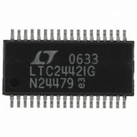
LTC2442IG#PBF Linear Technology, LTC2442IG#PBF Datasheet - Page 14

LTC2442IG#PBF
Manufacturer Part Number
LTC2442IG#PBF
Description
IC ADC 24BIT 4CH 36-SSOP
Manufacturer
Linear Technology
Datasheet
1.LTC2442CGPBF.pdf
(32 pages)
Specifications of LTC2442IG#PBF
Number Of Bits
24
Sampling Rate (per Second)
8k
Data Interface
MICROWIRE™, Serial, SPI™
Number Of Converters
1
Power Dissipation (max)
50mW
Voltage Supply Source
Single Supply
Operating Temperature
-40°C ~ 85°C
Mounting Type
Surface Mount
Package / Case
36-SSOP (0.200", 5.30mm Width)
Lead Free Status / RoHS Status
Lead free / RoHS Compliant
Available stocks
Company
Part Number
Manufacturer
Quantity
Price
APPLICATIO S I FOR ATIO
LTC2442
Chip Select Input (CS)
The active LOW chip select, CS (Pin 35), is used to test the
conversion status and to enable the data output transfer
as described in the previous sections.
In addition, the CS signal can be used to trigger a new
conversion cycle before the entire serial data transfer has
been completed. The LTC2442 will abort any serial data
transfer in progress and start a new conversion cycle
anytime a LOW-to-HIGH transition is detected at the CS
pin after the converter has entered the data output state.
Serial Data Input (SDI)
The serial data input (SDI, Pin 33) is used to select the
speed/resolution and input channel of the LTC2442. SDI is
programmed by a serial input data stream under the control
of SCK during the data output cycle, see Figure 3.
Initially, after powering up, the device performs a conver-
sion with SEL
nominally 879Hz), and 1X speedup mode (no Latency).
Once this fi rst conversion is complete, the device enters
the sleep state and is ready to output the conversion
result and receive the serial data input stream program-
ming the speed/resolution and input channel for the next
conversion. At the conclusion of each conversion cycle,
the device enters this state.
In order to change the speed/resolution or input channel,
the fi rst three bits shifted into the device are 101. This is
compatible with the programming sequence of all LTC
multichannel differential input ΔΣ ADCs. If the sequence
is set to 000 or 100, the following input data is ignored
(don’t care) and the previously selected speed/resolution
and channel remain valid for the next conversion. Combi-
nations other than 101, 100, and 000 of the three control
bits should be avoided.
14
+
= CH0, SEL
U
–
U
= CH1, OSR = 256 (output rate
W
U
If the fi rst three bits shifted into the device are 101, then
the following fi ve bits select the input channel for the fol-
lowing conversion (see Tables 3 and 4). The next fi ve bits
select the speed/resolution and mode 1X (no Latency) 2X
(double output rate with one conversion latency), see Table
4. If these fi ve bits are set to all 0’s, the previous speed
remains selected for the next conversion. This is useful
in applications requiring a fi xed output rate/resolution but
need to change the input channel.
When an update operation is initiated the fi rst three bits
are 101. The following fi ve bits are the channel address.
The fi rst bit, SGL, determines if the input selection is dif-
ferential (SGL = 0) or single-ended (SGL = 1). For SGL =
0, two adjacent channels can be selected to form a dif-
ferential input. For SGL = 1, one of 4 channels is selected
as the positive input. The negative input is COM for all
single ended operations. The next 4-bits (ODD, A2, A1,
A0) determine which channel is selected and its polarity,
(see Table 3). In order to remain software compatible with
LTCs other multi-channel ΔΣ ADCs, A2 and A1 are unused
and should be set low.
Speed Multiplier Mode
In addition to selecting the speed/resolution, a speed
multiplier mode is used to double the output rate while
maintaining the selected resolution. The last bit of the
5-bit speed/resolution control word (TWOX, see Table 4)
determines if the output rate is 1X (no speed increase) or
2X (double the selected speed).
While operating in the 1X mode, the device combines two
internal conversions for each conversion result in order
to remove the ADC offset. Every conversion cycle, the
offset and offset drift are transparently calibrated greatly
simplifying the user interface. The resulting conversion
result has no latency. The fi rst conversion following a newly
2442f


