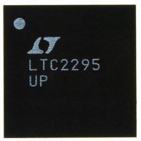
LTC2295IUP#PBF Linear Technology, LTC2295IUP#PBF Datasheet - Page 14

LTC2295IUP#PBF
Manufacturer Part Number
LTC2295IUP#PBF
Description
IC ADC DUAL 14BIT 10MSPS 64QFN
Manufacturer
Linear Technology
Datasheet
1.LTC2295IUPPBF.pdf
(24 pages)
Specifications of LTC2295IUP#PBF
Number Of Bits
14
Sampling Rate (per Second)
10M
Data Interface
Parallel
Number Of Converters
2
Power Dissipation (max)
138mW
Voltage Supply Source
Single Supply
Operating Temperature
-40°C ~ 85°C
Mounting Type
Surface Mount
Package / Case
64-WFQFN, Exposed Pad
Lead Free Status / RoHS Status
Lead free / RoHS Compliant
Available stocks
Company
Part Number
Manufacturer
Quantity
Price
The 25Ω resistors and 12pF capacitor on the analog inputs
serve two purposes: isolating the drive circuitry from the
sample-and-hold charging glitches and limiting the
wideband noise at the converter input.
LTC2295
APPLICATIO S I FOR ATIO
Figure 4 demonstrates the use of a differential amplifier to
convert a single ended input signal into a differential input
signal. The advantage of this method is that it provides low
frequency input response; however, the limited gain band-
width of most op amps will limit the SFDR at high input
frequencies.
Figure 5 shows a single-ended input circuit. The imped-
ance seen by the analog inputs should be matched. This
circuit is not recommended if low distortion is required.
14
ANALOG
ANALOG
INPUT
INPUT
Figure 4. Differential Drive with an Amplifier
0.1µF
DIFFERENTIAL
+
CM
–
HIGH SPEED
Figure 5. Single-Ended Drive
AMPLIFIER
+
–
U
1k
25Ω
25Ω
U
1k
0.1µF
25Ω
25Ω
12pF
12pF
2.2µF
2.2µF
W
V
A
A
CM
IN
IN
V
A
A
CM
IN
IN
+
–
+
–
LTC2295
LTC2295
U
2295 F04
2295 F05
TIE TO V
TIE TO V
Reference Operation
Figure 6 shows the LTC2295 reference circuitry consisting
of a 1.5V bandgap reference, a difference amplifier and
switching and control circuit. The internal voltage refer-
ence can be configured for two pin selectable input ranges
of 2V (±1V differential) or 1V (±0.5V differential). Tying the
SENSE pin to V
pin to V
The 1.5V bandgap reference serves two functions: its
output provides a DC bias point for setting the common
mode voltage of any external input circuitry; additionally,
the reference is used with a difference amplifier to gener-
ate the differential reference levels needed by the internal
ADC circuitry. An external bypass capacitor is required for
the 1.5V reference output, V
frequency low impedance path to ground for internal and
external circuitry.
RANGE = 2 • V
CM
0.5V < V
DD
FOR 2V RANGE;
FOR 1V RANGE;
CM
2.2µF
1µF
1µF
1.5V
SENSE
SENSE
selects the 1V range.
Figure 6. Equivalent Reference Circuit
< 1V
FOR
DD
selects the 2V range; tying the SENSE
2.2µF
SENSE
0.1µF
REFH
REFL
V
CM
LTC2295
CONTROL
DETECT
4Ω
RANGE
AND
CM
. This provides a high
1.5V BANDGAP
DIFF AMP
REFERENCE
INTERNAL ADC
HIGH REFERENCE
INTERNAL ADC
LOW REFERENCE
1V
BUFFER
0.5V
2295 F06
2295fa


