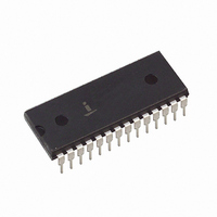
HI3-574AKN-5Z Intersil, HI3-574AKN-5Z Datasheet - Page 11

HI3-574AKN-5Z
Manufacturer Part Number
HI3-574AKN-5Z
Description
IC ADC 12BIT 40KSPS 28-PDIP
Manufacturer
Intersil
Datasheet
1.HI3-574AKN-5Z.pdf
(18 pages)
Specifications of HI3-574AKN-5Z
Number Of Bits
12
Sampling Rate (per Second)
40k
Data Interface
Parallel
Number Of Converters
1
Power Dissipation (max)
720mW
Voltage Supply Source
Dual ±
Operating Temperature
0°C ~ 75°C
Mounting Type
Through Hole
Package / Case
28-DIP (0.600", 15.24mm)
Lead Free Status / RoHS Status
Lead free / RoHS Compliant
Available stocks
Company
Part Number
Manufacturer
Quantity
Price
Company:
Part Number:
HI3-574AKN-5Z
Manufacturer:
Intersil
Quantity:
65
Company:
Part Number:
HI3-574AKN-5Z
Manufacturer:
Intersil
Quantity:
145
If the application calls for a Sample/Hold to precede the
converter, it should be noted that not all Sample/Holds are
compatible with the HI-574A in the manner described above.
These will require an additional wideband buffer amplifier to
lower their output impedance. A simpler solution is to use the
Intersil HA-5320 Sample/Hold, which was designed for use
with the HI-574A.
†
†
-15V
ANALOG
When driving the 20V (pin 14) input, minimize capacitance on pin 13.
When driving the 20V (pin 14) input, minimize capacitance on pin 13.
INPUTS
ANALOG
INPUTS
100Ω
100K
0V TO +10V
0V TO +20V
OFFSET
±10V
±5V
100K
R1
FIGURE 1. UNIPOLAR CONNECTIONS
FIGURE 2. BIPOLAR CONNECTIONS
R1
R2
100Ω
100Ω
R2
+15V
100Ω
OFFSET
GAIN
GAIN
11
2 12/8
3 CS
4 A
5 R/C
6 CE
10 REF IN
8 REF OUT
12 BIP OFF
13 10V
14 20V
9 ANA
2 12/8
3 CS
4 A
5 R/C
6 CE
10 REF IN
8 REF OUT
12 BIP OFF
13 10V
14 20V
9 ANA
COM
COM
O
O
IN
IN
IN
IN
†
†
MIDDLE BITS
DIG COM 15
MIDDLE BITS
DIG COM 15
HIGH BITS
LOW BITS
HIGH BITS
LOW BITS
-15V 11
STS 28
+15V 7
+15V 7
-15V 11
+5V 1
24-27
20-23
16-19
STS 28
+5V 1
24-27
20-23
16-19
HI-574A, HI-674A
Range Connections and Calibration Procedures
The HI-X74A is a “complete” A/D converter, meaning it is fully
operational with addition of the power supply voltages, a Start
Convert signal, and a few external components as shown in
Figures 1 and 2. Nothing more is required for most
applications.
Whether controlled by a processor or operating in the
stand-alone mode, the HI-X74A offers four standard input
ranges: 0V to +10V, 0V to +20V, ±5V and ±10V. The
maximum errors for gain and offset are listed under
Specifications. If required, however, these errors may be
adjusted to zero as explained below. Power supply and
ground connections have been discussed in an earlier
section.
Unipolar Connections and Calibration
Refer to Figure 1. The resistors shown (see Note below)
are for calibration of offset and gain. If this is not required,
replace R2 with a 50Ω, 1% metal film resistor and remove
the network on pin 12. Connect pin 12 to pin 9. Then,
connect the analog signal to pin 13 for the 0V to 10V range,
or to pin 14 for the 0V to 20V range. Inputs to +20V (5V
over the power supply) are no problem - the converter
operates normally.
Calibration consists of adjusting the converter’s most
negative output to its ideal value (offset adjustment), then,
adjusting the most positive output to its ideal value (gain
adjustment). To understand the procedure, note that in
principle, one is setting the output with respect to the
midpoint of an increment of analog input, as denoted by
two adjacent code changes. Nominal value of an increment
is one LSB. However, this approach is impractical because
nothing “happens” at a midpoint to indicate that an
adjustment is complete. Therefore, calibration is performed
in terms of the observable code changes instead of the
midpoint between code changes.
For example, midpoint of the first LSB increment should be
positioned at the origin, with an output code of all 0’s. To do
this, apply an input of +
+2.44mV for the 20V range). Adjust the Offset potentiometer
R1 until the first code transition flickers between
0000 0000 0000 and 0000 0000 0001.
Next, perform a Gain Adjust at positive full scale. Again, the
ideal input corresponding to the last code change is applied.
This is 1
10V range; +19.9927V for 20V range). Adjust the Gain
potentiometer R2 for flicker between codes 1111 1111 1110
and 1111 1111 1111.
Bipolar Connections and Calibration
Refer to Figure 2. The gain and offset errors listed under
Specifications may be adjusted to zero using
potentiometers R1 and R2 (see Note below). If this isn’t
1
/
2
LSBs below the nominal full scale (+9.9963V for
1
/
2
LSB (+1.22mV for the 10V range;
August 7, 2008
FN3096.6


