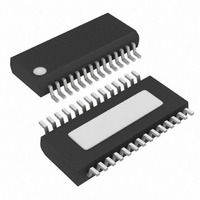
MAX1091BEEI+ Maxim Integrated Products, MAX1091BEEI+ Datasheet - Page 13

MAX1091BEEI+
Manufacturer Part Number
MAX1091BEEI+
Description
IC ADC 10BIT 250KSPS 28-QSOP
Manufacturer
Maxim Integrated Products
Datasheet
1.MAX1093BEEG.pdf
(20 pages)
Specifications of MAX1091BEEI+
Number Of Bits
10
Sampling Rate (per Second)
250k
Data Interface
Parallel
Number Of Converters
1
Power Dissipation (max)
667mW
Voltage Supply Source
Single Supply
Operating Temperature
-40°C ~ 85°C
Mounting Type
Surface Mount
Package / Case
28-QSOP
Number Of Adc Inputs
8
Architecture
SAR
Conversion Rate
250 KSPs
Resolution
10 bit
Input Type
Differential
Interface Type
Parallel
Voltage Reference
Internal 2.5 V or External
Supply Voltage (max)
3 V
Maximum Power Dissipation
762 mW
Maximum Operating Temperature
+ 85 C
Mounting Style
SMD/SMT
Minimum Operating Temperature
- 40 C
Lead Free Status / RoHS Status
Lead free / RoHS Compliant
The MAX1091/MAX1093 operate with either an internal
or an external clock. Control bits D6 and D7 select
either internal or external clock mode. The parts retain
the last-requested clock mode if a power-down mode is
selected in the current input word. For both internal and
external clock modes, internal or external acquisition
can be used. At power-up, the MAX1091/MAX1093
enter the default external clock mode.
Select internal clock mode to release the µP from the
burden of running the SAR conversion clock. To select
this mode, bit D7 of the control byte must be set to 1
and D6 must be set to 0. The internal clock frequency is
then selected, resulting in a conversion time of 3.6µs.
When using the internal clock mode, tie the CLK pin
either high or low to prevent the pin from floating.
To select the external clock mode, bits D6 and D7 of
the control byte must be set to one. Figure 6 shows the
clock and WR timing relationship for internal (Figure 6a)
and external (Figure 6b) acquisition modes with an
external clock. For proper operation, a 100kHz to
4.8MHz clock frequency with 30% to 70% duty cycle is
recommended. Operating the MAX1091/MAX1093 with
clock frequencies lower than 100kHz is not recom-
mended, because it causes a voltage droop across the
Figure 6a. External Clock and WR Timing (Internal Acquisition Mode)
CLK
CLK
WR
WR
with +2.5V Reference and Parallel Interface
t
CWH
______________________________________________________________________________________
ACQMOD = "0"
250ksps, +3V, 8-/4-Channel, 10-Bit ADCs
ACQMOD = "0"
Selecting Clock Mode
ACQUISITION STARTS
External Clock Mode
Internal Clock Mode
ACQUISITION STARTS
t
CWS
t
CH
t
CP
t
CL
WR GOES HIGH WHEN CLK IS HIGH.
WR GOES HIGH WHEN CLK IS LOW.
ACQUISITION ENDS
ACQUISITION ENDS
hold capacitor in the T/H stage that results in degraded
performance.
Input (control byte) and output data are multiplexed on
a three-state parallel interface. This parallel interface
(I/O) can easily be interfaced with standard µPs. The
signals CS, WR, and RD control the write and read
operations. CS represents the chip select signal, which
enables a µP to address the MAX1091/MAX1093 as an
I/O port. When high, CS disables the CLK WR and RD
inputs and forces the interface into a high-impedance
(high-Z) state.
The control byte is latched into the device on pins
D7–D0 during a write command. Table 2 shows the
control byte format.
The output format for both the MAX1091/MAX1093 is
binary in unipolar mode and two’s complement in bipo-
lar mode. When reading the output data, CS and RD
must be low. When HBEN = 0, the lower 8 bits are read.
With HBEN = 1, the upper 2 bits are available and the
output data bits D7–D2 are set either low in unipolar
mode or set to the value of the MSB in bipolar mode
(Table 5).
CONVERSION STARTS
CONVERSION STARTS
Digital Interface
Output Format
Input Format
13


