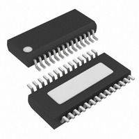
MAX1091BEEI+ Maxim Integrated Products, MAX1091BEEI+ Datasheet - Page 2

MAX1091BEEI+
Manufacturer Part Number
MAX1091BEEI+
Description
IC ADC 10BIT 250KSPS 28-QSOP
Manufacturer
Maxim Integrated Products
Datasheet
1.MAX1093BEEG.pdf
(20 pages)
Specifications of MAX1091BEEI+
Number Of Bits
10
Sampling Rate (per Second)
250k
Data Interface
Parallel
Number Of Converters
1
Power Dissipation (max)
667mW
Voltage Supply Source
Single Supply
Operating Temperature
-40°C ~ 85°C
Mounting Type
Surface Mount
Package / Case
28-QSOP
Number Of Adc Inputs
8
Architecture
SAR
Conversion Rate
250 KSPs
Resolution
10 bit
Input Type
Differential
Interface Type
Parallel
Voltage Reference
Internal 2.5 V or External
Supply Voltage (max)
3 V
Maximum Power Dissipation
762 mW
Maximum Operating Temperature
+ 85 C
Mounting Style
SMD/SMT
Minimum Operating Temperature
- 40 C
Lead Free Status / RoHS Status
Lead free / RoHS Compliant
ABSOLUTE MAXIMUM RATINGS
V
V
CH0–CH7, COM to GND ............................-0.3V to (V
REF, REFADJ to GND ................................-0.3V to (V
Digital Inputs to GND ...............................................-0.3V to +6V
Digital Outputs (D0–D9, INT) to GND.....-0.3V to (V
250ksps, +3V, 8-/4-Channel, 10-Bit ADCs
with +2.5V Reference and Parallel Interface
Stresses beyond those listed under “Absolute Maximum Ratings” may cause permanent damage to the device. These are stress ratings only, and functional
operation of the device at these or any other conditions beyond those indicated in the operational sections of the specifications is not implied. Exposure to
absolute maximum rating conditions for extended periods may affect device reliability.
ELECTRICAL CHARACTERISTICS
(V
cycle), T
2
DC ACCURACY (Note 1)
DYNAMIC SPECIFICATIONS (f
CONVERSION RATE
DD
LOGIC
Resolution
Relative Accuracy (Note 2)
Differential Nonlinearity
Offset Error
Gain Error (Note 3)
Gain Temperature Coefficient
Channel-to-Channel Offset
Matching
Signal-to-Noise Plus Distortion
Total Harmonic Distortion
(including 5th-order harmonic)
Spurious-Free Dynamic Range
Intermodulation Distortion
Channel-to-Channel Crosstalk
Full-Linear Bandwidth
Full-Power Bandwidth
Conversion Time (Note 5)
Track/Hold Acquisition Time
Aperture Delay
Aperture Jitter
External Clock Frequency
Duty Cycle
DD
_______________________________________________________________________________________
to GND ..............................................................-0.3V to +6V
= V
to GND.........................................................-0.3V to +6V
A
LOGIC
PARAMETER
= T
MIN
= +2.7V to +3.6V, COM = GND, REFADJ = V
to T
MAX
, unless otherwise noted. Typical values are at T
IN(sine wave)
SYMBOL
SINAD
t
SFDR
CONV
t
RES
DNL
THD
f
IMD
ACQ
INL
CLK
= 50kHz, V
MAX109_A
MAX109_B
No missing codes over temperature
f
f
SINAD > 56dB
-3dB rolloff
External clock mode
External acquisition/internal clock mode
Internal acquisition/internal clock mode
External acquisition or external clock mode
External acquisition or external clock mode
Internal acquisition/internal clock mode
IN1
IN
LOGIC
= 125kHz, V
= 49kHz, f
DD
DD
+ 0.3V)
+ 0.3V)
+ 0.3V)
IN
= 2.5V
DD
IN2
IN
CONDITIONS
, V
P-P
= 2.5V
= 52kHz
REF
, 250ksps, external f
Continuous Power Dissipation (T
Operating Temperature Ranges
Storage Temperature Range .............................-65°C to +150°C
Lead Temperature (soldering, 10s) .................................+300°C
= +2.5V, 4.7µF capacitor at REF pin, f
24-Pin QSOP (derate 9.5mW/°C above +70°C) ...........762mW
28-Pin QSOP (derate 8.00mW/°C above +70°C) .........667mW
MAX1091_C_ _/MAX1093_C_ _ ...........................0°C to +70°C
MAX1091_E_ _/MAX1093_E_ _ ........................-40°C to +85°C
P-P
A
(Note 4)
= +25°C.)
CLK
= 4.8MHz, bipolar input mode)
MIN
3.3
2.5
3.2
0.1
10
30
A
= +70°C)
<200
±2.0
±0.1
TYP
<50
250
-72
-78
3.0
3.6
60
72
76
50
CLK
3
= 4.8MHz (50% duty
MAX
±0.5
625
3.5
4.1
4.8
±1
±1
±2
±2
70
ppm/°C
UNITS
MHz
MHz
LSB
LSB
LSB
LSB
LSB
Bits
kHz
dB
dB
dB
dB
dB
µs
ns
ns
ps
%


