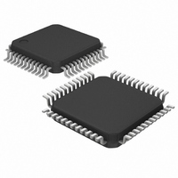
MAX1421ECM+D Maxim Integrated Products, MAX1421ECM+D Datasheet

MAX1421ECM+D
Specifications of MAX1421ECM+D
Related parts for MAX1421ECM+D
MAX1421ECM+D Summary of contents
Page 1
... CCD Pixel Processing Data Acquisition Radar IF and Baseband Digitization Functional Diagram appears at end of data sheet. ________________________________________________________________ Maxim Integrated Products For pricing, delivery, and ordering information, please contact Maxim/Dallas Direct! at 1-888-629-4642, or visit Maxim’s website at www.maxim-ic.com. with Internal Reference ♦ Single 3.3V Power Supply ♦ ...
Page 2
Low-Power ADC with Internal Reference ABSOLUTE MAXIMUM RATINGS AGND ..............................................-0. DGND..............................................-0. DGND to AGND.....................................................-0.3V to +0.3V INP, INN, REFP, REFN, REFIN, ...
Page 3
Low-Power ADC ELECTRICAL CHARACTERISTICS (continued 3.3V, AGND = DGND = 0, V AVDD DVDD f = 40MHz (50% duty cycle), digital output load C CLK by design and characterization. Typical values are at ...
Page 4
Low-Power ADC with Internal Reference ELECTRICAL CHARACTERISTICS (continued 3.3V, AGND = DGND = 0, V AVDD DVDD f = 40MHz (50% duty cycle), digital output load C CLK by design and characterization. Typical ...
Page 5
Low-Power ADC ELECTRICAL CHARACTERISTICS (continued 3.3V, AGND = DGND = 0, V AVDD DVDD f = 40MHz (50% duty cycle), digital output load C CLK by design and characterization. Typical values are at ...
Page 6
Low-Power ADC with Internal Reference ( 3.3V, AGND = DGND = 0, V AVDD DVDD load C = 10pF unless otherwise noted. Typical values are ...
Page 7
Low-Power ADC ( 3.3V, AGND = DGND = 0, V AVDD DVDD load C = 10pF unless otherwise noted. Typical values are MIN MAX, SPURIOUS-FREE ...
Page 8
Low-Power ADC with Internal Reference ( 3.3V, AGND = DGND = 0, V AVDD DVDD load C = 10pF unless otherwise noted. Typical values are ...
Page 9
Low-Power ADC PIN NAME 12, 13, AGND Analog Ground. Connect all return paths for analog signals to AGND. 16, 19, 41 10, Analog Supply Voltage. For optimum performance bypass ...
Page 10
Low-Power ADC with Internal Reference Detailed Description The MAX1421 uses a 12-stage, fully-differential, pipe- lined architecture (Figure 1) that allows for high-speed conversion while minimizing power consumption. Each sample moves through a pipeline stage every half- clock-cycle. ...
Page 11
Low-Power ADC Figure 3. Unbuffered External Reference Drive—Internal Reference Disabled The MAX1421 provides three modes of reference oper- ation: • Internal reference mode • Buffered external reference mode • Unbuffered external reference mode ...
Page 12
Low-Power ADC with Internal Reference INP ADC INN A VDD 10kΩ CLK 10kΩ CLK AGND Figure 4. Simplified Clock Input Circuit Figure 4 shows a simplified model of the clock input cir- cuit. This circuit consists of ...
Page 13
Low-Power ADC N ANALOG INPUT CLK t DO CLK DATA OUTPUT Figure 6. System and Output Timing Diagram Using Transformer Coupling An RF transformer (Figure 8) provides an excellent solu- tion to convert a ...
Page 14
Low-Power ADC with Internal Reference 300Ω 300Ω +5V 0.1µF INPUT MAX4108 0.1µF -5V 300Ω 300Ω Figure 7. Typical Application Circuit for Single-Ended to Differential Conversion error specification of less than 1LSB guarantees no missing codes. Dynamic Parameter ...
Page 15
Low-Power ADC V IN Figure 8. Using a Transformer for AC-Coupling V IN MAX4108 Figure 9. Single-Ended AC-Coupled Input Signal CLK CLK ANALOG INPUT SAMPLED DATA (T/H) TRACK HOLD T/H Figure 10. Track-and-Hold ...
Page 16
Low-Power ADC with Internal Reference Total Harmonic Distortion (THD) THD is typically the ratio of the RMS sum of the first four harmonics of the input signal to the fundamental itself. This is expressed as: ( ...
Page 17
... Maxim cannot assume responsibility for use of any circuitry other than circuitry entirely embodied in a Maxim product. No circuit patent licenses are implied. Maxim reserves the right to change the circuitry and specifications without notice at any time. 17 ____________________Maxim Integrated Products, 120 San Gabriel Drive, Sunnyvale, CA 94086 408-737-7600 © 2006 Maxim Integrated Products with Internal Reference Package Information PACKAGE OUTLINE, 32/48L LQFP, 7x7x1 ...


