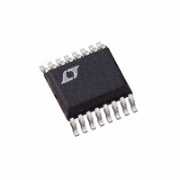
LTC2435CGN Linear Technology, LTC2435CGN Datasheet - Page 15

LTC2435CGN
Manufacturer Part Number
LTC2435CGN
Description
IC ADC DIFF I/REF 20BIT 16-SSOP
Manufacturer
Linear Technology
Datasheet
1.LTC2435-1CGN.pdf
(40 pages)
Specifications of LTC2435CGN
Number Of Bits
20
Sampling Rate (per Second)
15
Data Interface
MICROWIRE™, Serial, SPI™
Number Of Converters
2
Power Dissipation (max)
1mW
Voltage Supply Source
Single Supply
Operating Temperature
0°C ~ 70°C
Mounting Type
Surface Mount
Package / Case
16-SSOP (0.150", 3.90mm Width)
Lead Free Status / RoHS Status
Contains lead / RoHS non-compliant
Available stocks
Company
Part Number
Manufacturer
Quantity
Price
Company:
Part Number:
LTC2435CGN
Manufacturer:
LT
Quantity:
10 000
Part Number:
LTC2435CGN
Manufacturer:
LTNEAR
Quantity:
20 000
Part Number:
LTC2435CGN#PBF
Manufacturer:
LINEAR/凌特
Quantity:
20 000
APPLICATIO S I FOR ATIO
tional to V
variation can be used to eliminate the effects. First, the
variation with respect to supply voltage is linear. Second,
the magnitude of the offset error decreases with de-
creased supply voltage. Third, the offset error in micro-
volts is almost independent with reference and therefore
–350
–400
–450
–500
–550
–600
–650
–700
–750
2.5
Table 2. LTC2435/LTC2435-1 Output Data Format
Differential Input Voltage
V
V
0.5 • V
0.25 • V
0.25 • V
0
–1LSB
– 0.25 • V
– 0.25 • V
– 0.5 • V
V
*The differential input voltage V
Figure 4. Offset vs V
IN
IN
IN
CC
3.0
* ≥ 0.5 • V
* < –0.5 • V
*
SDO
SCK
CS
(see Figure 4), several characteristics of this
REF
REF
REF
REF
SLEEP
3.5
REF
REF
** – 1LSB
**
** – 1LSB
**
Hi-Z
**
** – 1LSB
REF
V
REF
CC
U
4.0
**
(V)
**
BIT 23
EOC
4.5
U
CC
REF
REF
V
V
F
T
O
A
IN
INCM
= GND
= 25°C
+
–
= 0V
5.0
= 2.5V
= GND
BIT 22
= GND
IN
“0”
2435 F04
= IN
5.5
Bit 23
W
EOC
0
0
0
0
0
0
0
0
0
0
+
– IN
BIT 21
–
SIG
–324
–325
–326
–327
–328
–329
–330
.
Bit 22
DMY
Figure 5. Offset vs Temperature
–45 –30
0
0
0
0
0
0
0
0
0
0
Figure 3. Output Data Timing
U
BIT 20
MSB
–15
Bit 21
DATA OUTPUT
SIG
1
1
1
1
1
0
0
0
0
0
TEMPERATURE (°C)
0
BIT 19
15
Bit 20
MSB
the offset in ppm is inverse proportional to reference
voltage. As a result, by tying V
supply can be reduced, see Figure 6. The variation with
supply is less than 15ppm over the entire 2.7V to 5.5V
supply range.
Frequency Rejection Selection LTC2435 (F
1
0
0
0
0
1
1
1
1
0
30
**The differential reference voltage V
45
V
V
V
V
F
O
CC
REF
IN
INCM
Bit 19
60
= GND
= 0V
= 5V
0
1
1
0
0
1
1
0
0
1
= 5V
= GND
75
2435 F05
BIT 5
90
Bit 18
LTC2435/LTC2435-1
0
1
0
1
0
1
0
1
0
1
–300
–305
–310
–315
–320
–325
–330
–335
–340
–345
–350
BIT 0
Figure 6. Offset vs V
LSB
Bit 17
2.5
0
1
0
1
0
1
0
1
0
1
CC
REF
3.0
CONVERSION
to V
= REF
…
…
…
…
…
…
…
…
…
…
…
–
3.5
V
REF
CC
+
2435 F03
– REF
and V
, the variation with
4.0
CC
Bit 0
REF
0
1
0
1
0
1
0
1
0
1
–
(V
.
O
(V)
REF
)
4.5
REF
REF
V
V
F
T
O
IN
INCM
A
= V
= GND
= 25°C
+
–
= 0V
15
5.0
= V
= GND
CC
= GND
24351fb
CC
2435 F06
)
5.5


