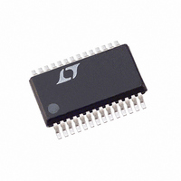
LTC2439-1CGN#TRPBF Linear Technology, LTC2439-1CGN#TRPBF Datasheet - Page 16

LTC2439-1CGN#TRPBF
Manufacturer Part Number
LTC2439-1CGN#TRPBF
Description
IC ADC 16BIT 16CH MCRPWR 28SSOP
Manufacturer
Linear Technology
Datasheet
1.LTC2439-1CGN.pdf
(28 pages)
Specifications of LTC2439-1CGN#TRPBF
Number Of Bits
16
Sampling Rate (per Second)
6.8
Data Interface
MICROWIRE™, Serial, SPI™
Number Of Converters
1
Power Dissipation (max)
1mW
Voltage Supply Source
Single Supply
Operating Temperature
0°C ~ 70°C
Mounting Type
Surface Mount
Package / Case
28-SSOP (0.150", 3.95mm Width)
Lead Free Status / RoHS Status
Lead free / RoHS Compliant
Available stocks
Company
Part Number
Manufacturer
Quantity
Price
(EXTERNAL)
APPLICATIO S I FOR ATIO
LTC2439-1
shift register. The input data is then shifted in via the SDI
pin on the rising edge of SCK (including the first rising
edge) and the output data is shifted out of the SDO pin on
each falling edge of SCK. EOC can be latched on the first
16
(EXTERNAL)
SDO
SCK
SDI
CS
SDO
SLEEP
SCK
SDI
CONVERSION
CS
OUTPUT
DATA
BIT 0
EOC
DON’T CARE
U
CONVERSION
Hi-Z
TEST EOC
DON’T CARE
U
Hi-Z
SLEEP
(OPTIONAL)
TEST EOC
BIT 18
(1)
EOC
Figure 7. External Serial Clock, Reduced Data Output Length
SLEEP
Hi-Z
W
BIT 17
(0)
“O”
Figure 8. External Serial Clock, CS = 0 Operation
(1)
BIT 18
EOC
EN
BIT 16
SIG
BIT 17
“O”
0.1V TO V
REFERENCE
U
(0)
ANALOG
INPUTS
VOLTAGE
SGL
BIT 15
0.1V TO V
1µF
REFERENCE
2.7V TO 5.5V
MSB
ANALOG
INPUTS
VOLTAGE
CC
1µF
2.7V TO 5.5V
•
•
•
•
•
•
BIT 16
11
12
21
28
10
SIG
CC
EN
9
1
8
ODD/
SIGN
BIT 14
V
REF
REF
CH0
CH7
CH8
CH15
COM
•
•
•
•
•
•
CC
LTC2439-1
•
•
•
•
•
•
11
12
21
28
10
9
1
8
+
–
V
REF
REF
CH0
CH7
CH8
CH15
COM
BIT 15
CC
MSB
LTC2439-1
•
•
•
•
•
•
SGL
rising edge of SCK. On the 19th falling edge of SCK, SDO
goes HIGH (EOC = 1) indicating a new conversion has
begun.
GND
+
–
SDO
SCK
A2
BIT 13
SDI
CS
F
O
DATA OUTPUT
GND
17
15
SDO
SCK
SDI
20
18
19
16
CS
F
BIT 14
O
ODD/
SIGN
17
15
BIT 12
A1
20
18
19
16
DATA OUTPUT
3-WIRE
SPI INTERFACE
BIT 13
A2
= EXTERNAL CLOCK SOURCE
= INTERNAL OSC/SIMULTANEOUS
4-WIRE
SPI INTERFACE
50Hz/60Hz REJECTION
A0
BIT 11
= EXTERNAL CLOCK SOURCE
= INTERNAL OSC/SIMULTANEOUS
50Hz/60Hz REJECTION
BIT 12
A1
BIT 11
DON’T CARE
A0
BIT 6
BIT 5
BIT 4
DON’T CARE
BIT 0
LSB
CONVERSION
Hi-Z
TEST EOC
CONVERSION
24391 F06
24391fa
24391 F07


