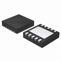
LTC2484CDD#PBF Linear Technology, LTC2484CDD#PBF Datasheet - Page 17

LTC2484CDD#PBF
Manufacturer Part Number
LTC2484CDD#PBF
Description
IC ADC 24BIT 10-DFN
Manufacturer
Linear Technology
Datasheet
1.LTC2484CDDTRPBF.pdf
(42 pages)
Specifications of LTC2484CDD#PBF
Number Of Bits
24
Sampling Rate (per Second)
6.8
Data Interface
MICROWIRE™, Serial, SPI™
Number Of Converters
1
Power Dissipation (max)
480µW
Voltage Supply Source
Single Supply
Operating Temperature
0°C ~ 70°C
Mounting Type
Surface Mount
Package / Case
10-WFDFN Exposed Pad
Number Of Elements
1
Resolution
24Bit
Architecture
Delta-Sigma
Sample Rate
0.0075KSPS
Input Polarity
Bipolar
Input Type
Voltage
Rated Input Volt
±2.75V
Differential Input
Yes
Power Supply Requirement
Single
Single Supply Voltage (typ)
3.3/5V
Single Supply Voltage (min)
2.7V
Single Supply Voltage (max)
5.5V
Dual Supply Voltage (typ)
Not RequiredV
Dual Supply Voltage (min)
Not RequiredV
Dual Supply Voltage (max)
Not RequiredV
Integral Nonlinearity Error
10ppm of Vref
Operating Temp Range
0C to 70C
Operating Temperature Classification
Commercial
Mounting
Surface Mount
Pin Count
10
Package Type
DFN EP
Input Signal Type
Differential
Lead Free Status / RoHS Status
Lead free / RoHS Compliant
Available stocks
Company
Part Number
Manufacturer
Quantity
Price
APPLICATIONS INFORMATION
an external serial clock. If the change occurs during the
conversion state, the result of the conversion in progress
may be outside specifi cations but the following conver-
sions will not be affected. If the change occurs during the
data output state and the converter is in the Internal SCK
mode, the serial clock duty cycle may be affected but the
serial data stream will remain valid.
Table 4 summarizes the duration of each state and the
achievable output data rate as a function of f
Table 4. LTC2484 State Duration
STATE
CONVERT
SLEEP
DATA OUTPUT
Figure 3. LTC2484 Nomal Mode Rejection When
Using an External Oscillator
–100
–105
–110
–115
–120
–125
–130
–135
–140
–80
–85
–90
–95
DEVIATION FROM NOTCH FREQUENCY f
–12
DIFFERENTIAL INPUT SIGNAL FREQUENCY
OPERATING MODE
Internal Oscillator
External Oscillator
Internal Serial Clock
External Serial Clock with
Frequency f
–8
–4
SCK
0
kHz
4
EOSC
8
/5120(%)
2484 F03
60Hz Rejection
50Hz Rejection
50Hz/60Hz Rejection
f
with Frequency f
(f
f
(Internal Oscillator)
f
Frequency f
O
O
O
EOSC
= External Oscillator
= LOW/HIGH
= External Oscillator with
12
O
/5120 Rejection)
.
EOSC
EOSC
kHz
kHz
Ease of Use
The LTC2484 data output has no latency, fi lter settling
delay or redundant data associated with the conversion
cycle. There is a one-to-one correspondence between the
conversion and the output data. Therefore, multiplexing
multiple analog voltages is easy.
The LTC2484 performs offset and full-scale calibrations
every conversion cycle. This calibration is transparent to
the user and has no effect on the cyclic operation described
above. The advantage of continuous calibration is extreme
stability of offset and full-scale readings with respect to
time, supply voltage change and temperature drift.
Power-Up Sequence
The LTC2484 automatically enters an internal reset
state when the power supply voltage V
approximately 2V. This feature guarantees the integrity
of the conversion result and of the serial interface mode
selection.
When the V
the converter creates an internal power-on reset (POR)
signal with a duration of approximately 4ms. The POR
signal clears all internal registers. Following the POR
signal, the LTC2484 starts a normal conversion cycle and
follows the succession of states described in Figure 1. The
DURATION
133ms, Output Data Rate ≤ 7.5 Readings/s for 1x Speed Mode
67ms, Output Data Rate ≤ 15 Readings/s for 2x Speed Mode
160ms, Output Data Rate ≤ 6.2 Readings/s for 1x Speed Mode
80ms, Output Data Rate ≤ 12.5 Readings/s for 2x Speed Mode
147ms, Output Data Rate ≤ 6.8 Readings/s for 1x Speed Mode
73.6ms, Output Data Rate ≤ 13.6 Readings/s for 2x Speed Mode
41036/f
1x Speed Mode
20556/
2x Speed Mode
As Long As CS = HIGH, After a Conversion is Complete
As Long As CS = LOW But Not Longer Than 0.83ms
(32 SCK Cycles)
As Long As CS = LOW But Not Longer Than 256/f
(32 SCK Cycles)
As Long As CS = LOW But Not Longer Than 32/f
(32 SCK Cycles)
fEOSC
EOSC
CC
voltage rises above this critical threshold,
s, Output Data Rate ≤ f
s, Output Data Rate ≤ f
EOSC
EOSC
/41036 Readings/s for
/20556 Readings/s for
LTC2484
CC
SCK
EOSC
drops below
ms
ms
17
2484fc


