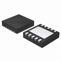
LTC2484CDD#PBF Linear Technology, LTC2484CDD#PBF Datasheet - Page 19

LTC2484CDD#PBF
Manufacturer Part Number
LTC2484CDD#PBF
Description
IC ADC 24BIT 10-DFN
Manufacturer
Linear Technology
Datasheet
1.LTC2484CDDTRPBF.pdf
(42 pages)
Specifications of LTC2484CDD#PBF
Number Of Bits
24
Sampling Rate (per Second)
6.8
Data Interface
MICROWIRE™, Serial, SPI™
Number Of Converters
1
Power Dissipation (max)
480µW
Voltage Supply Source
Single Supply
Operating Temperature
0°C ~ 70°C
Mounting Type
Surface Mount
Package / Case
10-WFDFN Exposed Pad
Number Of Elements
1
Resolution
24Bit
Architecture
Delta-Sigma
Sample Rate
0.0075KSPS
Input Polarity
Bipolar
Input Type
Voltage
Rated Input Volt
±2.75V
Differential Input
Yes
Power Supply Requirement
Single
Single Supply Voltage (typ)
3.3/5V
Single Supply Voltage (min)
2.7V
Single Supply Voltage (max)
5.5V
Dual Supply Voltage (typ)
Not RequiredV
Dual Supply Voltage (min)
Not RequiredV
Dual Supply Voltage (max)
Not RequiredV
Integral Nonlinearity Error
10ppm of Vref
Operating Temp Range
0C to 70C
Operating Temperature Classification
Commercial
Mounting
Surface Mount
Pin Count
10
Package Type
DFN EP
Input Signal Type
Differential
Lead Free Status / RoHS Status
Lead free / RoHS Compliant
Available stocks
Company
Part Number
Manufacturer
Quantity
Price
APPLICATIONS INFORMATION
V
Outside this range, the converter indicates the overrange
or the underrange condition using distinct output codes.
Since the differential input current cancellation does not
rely on an on-chip buffer, current cancellation as well as
DC performance is maintained rail-to-rail.
Input signals applied to IN
300mV below ground and above V
fault current, resistors of up to 5k may be added in series
with the IN
of the devices. The effect of the series resistance on the
converter accuracy can be evaluated from the curves
presented in the Input Current/Reference Current sections.
In addition, series resistors will introduce a temperature
dependent offset error due to the input leakage current.
A 1nA input leakage current will develop a 1ppm offset
error on a 5k resistor if V
strong temperature dependency.
SERIAL INTERFACE TIMING MODES
The LTC2484’s 4-wire interface is SPI and MICROWIRE
compatible. This interface offers several fl exible modes
of operation. These include internal/external serial clock,
3- or 4-wire I/O, single cycle or continuous conversion. The
following sections describe each of these serial interface
timing modes in detail. In all these cases, the converter
can use the internal oscillator (f
or an external oscillator connected to the f
Table 5 for a summary.
Table 5. LTC2484 Interface Timing Modes
CONFIGURATION
External SCK, Single Cycle Conversion
External SCK, 3-Wire I/O
Internal SCK, Single Cycle Conversion
Internal SCK, 3-Wire I/O, Continuous Conversion
IN
= IN
+
– IN
+
and IN
–
, from –FS to +FS where FS = 0.5 • V
–
pins without affecting the performance
REF
+
and IN
= 5V. This error has a very
O
CC
= LOW or f
–
. In order to limit any
pins may extend by
O
pin. Refer to
O
SOURCE
External
External
Internal
Internal
= HIGH)
SCK
REF
.
External Serial Clock, Single Cycle Operation
(SPI/MICROWIRE Compatible)
This timing mode uses an external serial clock to shift
out the conversion result and a CS signal to monitor and
control the state of the conversion cycle (see Figure 5).
The serial clock mode is selected on the falling edge of CS.
To select the external serial clock mode, the serial clock
pin (SCK) must be LOW during each CS falling edge.
The serial data output pin (SDO) is Hi-Z as long as CS is
HIGH. At any time during the conversion cycle, CS may be
pulled LOW in order to monitor the state of the converter.
While CS is pulled LOW, EOC is output to the SDO pin.
EOC = 1 while a conversion is in progress and EOC = 0
if the device is in the sleep state. Independent of CS, the
device automatically enters the low power sleep state once
the conversion is complete.
When the device is in the sleep state, its conversion result
is held in an internal static shift register. The device remains
in the sleep state until the fi rst rising edge of SCK is seen
while CS is LOW. The input data is then shifted in via the
SDI pin on the rising edge of SCK (including the fi rst rising
edge) and the output data is shifted out of the SDO pin on
each falling edge of SCK. This enables external circuitry
to latch the output on the rising edge of SCK. EOC can be
latched on the fi rst rising edge of SCK and the last bit of
the conversion result can be latched on the 32nd rising
edge of SCK. On the 32nd falling edge of SCK, the device
begins a new conversion. SDO goes HIGH (EOC = 1)
indicating a conversion is in progress.
CYCLE CONTROL
CONVERSION
CS and SCK
Continuous
SCK
CS↓
DATA OUTPUT
CS and SCK
CONTROL
Internal
SCK
CS↓
LTC2484
and WAVEFORMS
CONNECTION
Figures 5, 6
Figures 8, 9
Figure 10
Figure 7
19
2484fc


