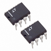
LTC1286CN8 Linear Technology, LTC1286CN8 Datasheet - Page 22

LTC1286CN8
Manufacturer Part Number
LTC1286CN8
Description
IC A/D CONV SAMPLING 12BIT 8-DIP
Manufacturer
Linear Technology
Datasheet
1.LTC1298CN8PBF.pdf
(24 pages)
Specifications of LTC1286CN8
Number Of Bits
12
Sampling Rate (per Second)
12.5k
Data Interface
MICROWIRE™, Serial, SPI™
Number Of Converters
1
Power Dissipation (max)
1.25mW
Voltage Supply Source
Single Supply
Operating Temperature
0°C ~ 70°C
Mounting Type
Through Hole
Package / Case
8-DIP (0.300", 7.62mm)
Lead Free Status / RoHS Status
Contains lead / RoHS non-compliant
Available stocks
Company
Part Number
Manufacturer
Quantity
Price
Company:
Part Number:
LTC1286CN8
Manufacturer:
NEC
Quantity:
184
(
D IN
DATA
/D
LTC1286/LTC1298
Interfacing to the Parallel Port of the INTEL 8051
Family
The Intel 8051 has been chosen to demonstrate the
interface between the LTC1298 and parallel port micro-
processors. Normally the CS, CLK and D
be generated on 3 port lines and the D
a 4th port line. This works very well. However, we will
demonstrate here an interface with the D
LTC1298 tied together as described in the SERIAL INTER-
FACE section. This saves one wire.
The 8051 first sends the start bit and MUX address to the
LTC1298 over the data line connected to P1.2. Then P1.2
is reconfigured as an input (by writing to it a one) and the
8051 reads back the 12-bit A/D result over the same data
line.
D
R2 B11 B10 B9
R3 B3 B2 B1 B0 0
22
TYPICAL APPLICATIONS
OUT
OUT
ANALOG
CLK
CS
INPUTS
)
FROM 1298 STORED IN 8501 RAM
MSB
LSB
AS IN INPUT AFTER THE 4TH RISING CLK
START
8051 P1.2 OUTPUTS DATA
AND BEFORE THE 4TH FALLING CLK
LTC1298
TO LTC1298
8051 P1.2 RECONFIGURED
D
CLK
OUT
D
CS
IN
B8 B7 B6 B5 B4
SGL/
DIFF
MUX ADDRESS
A/D RESULT
ODD/
SIGN
0
MSBF BIT LATCHED
INTO LTC1298
MSBF
0
U
OUT
IN
P1.4
P1.3
P1.2
0
IN
N
and D
signal read on
signals would
LTC1286/98 TA01
8051
B11
OUT
LTC1298 TAKES CONTROL OF DATA
LINE ON 4TH FALLING CLK
of the
B10
B9
LABEL
LOOP 1
LOOP 2
LOOP 3
LOOP 4
LTC1298 SENDS A/D RESULT
B8
BACK TO 8051 P1.2
B7
MNEMONIC
MOV
SETB
CLR
MOV
RLC
CLR
MOV
SETB
DJNZ
MOV
CLR
MOV
MOV
RLC
SETB
CLR
DJNZ
MOV
CLR
MOV
MOV
RLC
SETB
CLR
DJNZ
MOV
RRC
DJNZ
MOV
SETB
B6
B5
C, P1.2
C, P1.2
A, #FFH
P1.4
P1.4
R4, #04
A
P1.3
P1.2, C
P1.3
R4, LOOP 1
P1, #04
P1.3
R4, #09
A
P1.3
P1.3
R4, LOOP 2
R2, A
A
R4, #04
A
P1.3
P1.3
R4, LOOP 3
R4, #04
A
R4, LOOP 4
R3, A
P1.4
OPERAND
B4
B3
COMMENTS
D
Make sure CS is high
CS goes low
Load counter
Rotate D
SCLK goes low
Output D
SCLK goes high
Next bit
Bit 2 becomes an input
SCLK goes low
Load counter
Read data bit into Carry
Rotate data bit into Acc.
SCLK goes high
SCLK goes low
Next bit
Store MSBs in R2
Clear Acc.
Load counter
Read data bit into Carry
Rotate data bit into Acc.
SCLK goes high
SCLK goes low
Next bit
Load counter
Rotate right into Acc.
Next Rotate
Store LSBs in R3
CS goes high
IN
B2
word for LTC1298
IN
IN
B1
bit into Carry
bit to LTC1298
B0
LTC1286/98 TA02


