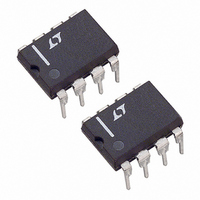
LTC1286CN8 Linear Technology, LTC1286CN8 Datasheet - Page 4

LTC1286CN8
Manufacturer Part Number
LTC1286CN8
Description
IC A/D CONV SAMPLING 12BIT 8-DIP
Manufacturer
Linear Technology
Datasheet
1.LTC1298CN8PBF.pdf
(24 pages)
Specifications of LTC1286CN8
Number Of Bits
12
Sampling Rate (per Second)
12.5k
Data Interface
MICROWIRE™, Serial, SPI™
Number Of Converters
1
Power Dissipation (max)
1.25mW
Voltage Supply Source
Single Supply
Operating Temperature
0°C ~ 70°C
Mounting Type
Through Hole
Package / Case
8-DIP (0.300", 7.62mm)
Lead Free Status / RoHS Status
Contains lead / RoHS non-compliant
Available stocks
Company
Part Number
Manufacturer
Quantity
Price
Company:
Part Number:
LTC1286CN8
Manufacturer:
NEC
Quantity:
184
LTC1286/LTC1298
SYMBOL
t
f
t
t
t
t
t
t
t
C
TYPICAL PERFORMANCE CHARACTERISTICS
AC CHARACTERISTICS
The
temperature range.
Note 1: Absolute maximum ratings are those values beyond which the life
of a device may be impaired.
Note 2: All voltage values are with respect to GND.
Note 3: These devices are specified at 5V. For 3V specified devices, see
LTC1285 and LTC1288.
Note 4: Increased leakage currents at elevated temperatures cause the S/H
to droop, therefore it is recommended that f
75kHz at 70 and f
Note 5: V
Note 6: Linearity error is specified between the actual end points of the
A/D transfer curve.
4
SMPL
SMPL (MAX)
CONV
dDO
dis
en
hDO
f
r
IN
1000
100
10
1
0.1k
Supply Current vs Sample Rate
denotes specifications which apply over the full operating
T
V
f
CC
CLK
A
CC
= 25°C
= 5V, V
= V
LTC1298
PARAMETER
Analog Input Sample Time
Maximum Sampling Frequency
Conversion Time
Delay Time, CLK to D
Delay Time, CS to D
Delay Time, CLK to D
Time Output Data Remains Valid After CLK
D
D
Input Capacitance
= 200kHz
OUT
OUT
REF
SAMPLE RATE (kHz)
CLK
1k
Fall Time
Rise Time
= 5V
REF
= 5V and CLK = 200kHz unless otherwise specified.
LTC1286
1kHz at 25 C.
10k
OUT
OUT
OUT
LT1286/98 G03
W
Hi-Z
Data Valid
Enable
100k
CLK
U
(Note 5)
120kHz at 85 C, f
400
300
200
450
350
250
–55
Supply Current vs Temperature
–35
CONDITIONS
See Operating Sequence
LTC1286
LTC1298
See Operating Sequence
See Test Circuits
See Test Circuits
See Test Circuits
C
See Test Circuits
See Test Circuits
Analog Inputs, On Channel
Analog Inputs, Off Channel
Digital Input
T
V
f
CLK
A
CC
LOAD
= 25°C
CLK
= V
= 200kHz
–15
REF
= 100pF
TEMPERATURE (°C)
5
= 5V
LTC1298 f
LTC1286 f
25
Note 7: Two on-chip diodes are tied to each reference and analog input
which will conduct for reference or analog input voltages one diode drop
below GND or one diode drop above V
bias of either diode for 4.5V V
reference or analog input does not exceed the supply voltage by more than
50mV the output code will be correct. To achieve an absolute 0V to 5V
input voltage range will therefore require a minimum supply voltage of
4.950V over initial tolerance, temperature variations and loading. For 5.5V
< V
reference and analog input range are greater than 5.55V, the output code
will not be guaranteed to be correct.
Note 8: The supply voltage range for the LTC1286 is from 4.5V to 9V, but
the supply voltage range for the LTC1298 is only from 4.5V to 5.5V.
Note 9: Recommended operating conditions
Note 10: Channel leakage current is measured after the channel selection.
45
CC
SMPL
SMPL
65
9V, reference and analog input range cannot exceed 5.55V. If
=12.5kHz
=11.1kHz
85 105
LT1286/98 G04
125
0.002
CC
35
30
25
20
15
10
5
1
0
12.5
11.1
MIN
Shutdown Supply Current vs Clock
Rate with CS High and CS Low
1
5.5V. This means that as long as the
T
V
CC
20
A
CC
. This spec allows 50mV forward
= 25°C
= V
40 60
TYP
REF
250
135
230
1.5
12
75
20
20
20
5
5
CS = V
= 5V
FREQUENCY (kHz)
80
CS = 0
(AFTER CONVERSION)
CC
MAX
600
300
200
100
75
75
120
140
CLK Cycles
CLK Cycles
160
LT1286/98 G01
UNITS
180 200
kHz
kHz
ns
ns
ns
ns
ns
ns
pF
pF
pF


