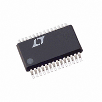
LTC1418IG Linear Technology, LTC1418IG Datasheet - Page 23

LTC1418IG
Manufacturer Part Number
LTC1418IG
Description
IC A/D CONV 14BIT SRL&PAR 28SSOP
Manufacturer
Linear Technology
Datasheet
1.LTC1418ACGPBF.pdf
(28 pages)
Specifications of LTC1418IG
Number Of Bits
14
Sampling Rate (per Second)
200k
Data Interface
Serial, Parallel
Number Of Converters
1
Power Dissipation (max)
21.5mW Unipolar; 31.5mW Bipolar
Voltage Supply Source
Dual ±
Operating Temperature
-40°C ~ 85°C
Mounting Type
Surface Mount
Package / Case
28-SSOP (0.200", 5.30mm Width)
Lead Free Status / RoHS Status
Contains lead / RoHS non-compliant
Available stocks
Company
Part Number
Manufacturer
Quantity
Price
Company:
Part Number:
LTC1418IG
Manufacturer:
LT
Quantity:
2 027
APPLICATIONS
serial port after transferring the serial output data by
tying it to the RD pin.
Figures 22 to 25 show several serial modes of operation,
demonstrating the flexibility of the LTC1418 serial port.
Serial Data Output During a Conversion
Using Internal Conversion Clock for Conversion and
Data Transfer. Figure 22 shows data from the previous
conversion being clocked out during the conversion with
the LTC1418 internal clock providing both the conversion
CS = 0, EXT/INT = 5
EXTCLKIN (= SCLK)
BUSY (= RD)
CONVST
D
OUT
(SAMPLE N)
t
dEXTCLKIN
t
Hi-Z
6
t
10
U
Figure 23. External Conversion Clock Selected. Data Transferred During Conversion Using
the External Clock (External Clock Drives Both EXTCLKIN and SCLK)
D13
1
t
5
INFORMATION
U
D12
2
CONVST
D11
3
EXTCLKIN
(= SCLK)
D
W
D10
OUT
24
4
D9
CONVST
5
V
D13
IL
LTC1418
D8
CS
EXTCLKIN
t
6
t
15
LEXTCLKIN
t
U
EXT/INT
25
14
BUSY
SCLK
D
DATA (N – 1)
OUT
D7
RD
RISING CLOCK
7
CAPTURE ON
t
CONV
26
19
20
D6
23
16
17
8
t
EXTCLKIN ( = SCLK)
5V
HEXTCLKIN
HOLD
D12
D5
BUSY (= RD)
9
FALLING CLOCK
clock and the SCLK. The internal clock has been optimized
for the fastest conversion time, consequently this mode
can provide the best overall speed performance. To select
an internal conversion clock, tie EXT/INT (Pin 20) low. The
internal clock appears on CLKOUT (Pin 18) which can be
tied to SCLK (Pin 17) to supply the SCLK.
Using External Clock for Conversion and Data Transfer.
In Figure 23, data from the previous conversion is output
during the conversion with an external clock providing
both the conversion clock and the shift clock. To select an
external conversion clock, tie EXT/INT high and apply the
t
D
13
CAPTURE ON
OUT
D4
10
D3
11
P OR DSP
D11
D2
12
V
V
1418 F23a
OH
OL
D1
13
D0
14
15
ZEROS
FILL
16
t
D13
7
(SAMPLE N + 1)
SAMPLE
t
8
Hi-Z
LTC1418
t
11
D13
1
DATA N
HOLD
23
D12
2
1418 F23b
D11
3


