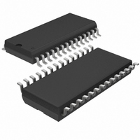
LTC1409CSW Linear Technology, LTC1409CSW Datasheet

LTC1409CSW
Specifications of LTC1409CSW
Available stocks
Related parts for LTC1409CSW
LTC1409CSW Summary of contents
Page 1
... SO Wide and SSOP Package O U PPLICATI S A Telecommunications Digital Signal Processing Multiplexed Data Acquisition Systems High Speed Data Acquisition Spectrum Analysis Imaging Systems , LTC and LT are registered trademarks of Linear Technology Corporation. O TYPICAL A PPLICATI 800kHz, 12-Bit Sampling A/D Converter LTC1409 DIFFERENTIAL ...
Page 2
... Consult factory for Military grade parts. With Internal Reference (Notes CONDITIONS 4.75V V 5.25V, – 5.25V High Between Conversions During Conversions – 2.5V < (– < 2. TOP VIEW ORDER PART NUMBER LTC1409CG LTC1409CSW 25 BUSY LTC1409IG 24 CS LTC1409ISW 23 CONVST SHDN 20 NAP/SLP 19 OGND PACKAGE 28-LEAD PLASTIC SO WIDE = 110 C/W (G) JA ...
Page 3
ACCURACY SYMBOL PARAMETER S/( Signal-to-Noise Plus Distortion Ratio 100kHz Input Signal (Note 12) THD Total Harmonic Distortion Peak Harmonic or Spurious Noise IMD Intermodulation Distortion Full Power Bandwidth Full Linear Bandwidth U U ...
Page 4
LTC1409 W U POWER REQUIRE E TS SYMBOL PARAMETER I Negative Supply Current SS Nap Mode Sleep Mode P Power Dissipation DISS Nap Mode Sleep Mode CHARACTERISTICS SYMBOL PARAMETER f Maximum Sampling Frequency SAMPLE(MAX) t ...
Page 5
CHARACTERISTICS Note 11: The falling CONVST edge starts a conversion. If CONVST returns high at a critical point during the conversion it can create small errors. For best results ensure that CONVST returns high either ...
Page 6
LTC1409 W U TYPICAL PERFORMANCE CHARACTERISTICS Integral Nonlinearity vs Output Code 1.00 0.50 0 –0.50 –1.00 0 512 1024 1536 2048 2560 3072 3584 4096 OUTPUT CODE Power Supply Feedthrough vs Ripple Frequency 0 –10 –20 –30 –40 –50 –60 ...
Page 7
CTIO S CONVST (Pin 23): Conversion Start Signal. This active low signal starts a conversion on its falling edge. CS (Pin 24): Chip Select. The input must be low for the ADC to recognize CONVST ...
Page 8
LTC1409 U U APPLICATIONS INFORMATION CONVERSION DETAILS The LTC1409 uses a successive approximation algorithm and an internal sample-and-hold circuit to convert an analog signal to a 12-bit parallel output. The ADC is complete with a precision reference and an internal ...
Page 9
U U APPLICATIONS INFORMATION Signal-to-Noise Ratio The signal-to-noise plus distortion ratio [S/(N + D)] is the ratio between the RMS amplitude of the fundamental input frequency to the RMS amplitude of all other frequency components at the A/D output. The ...
Page 10
LTC1409 U U APPLICATIONS INFORMATION 0 –20 –40 –60 fb – fa 2fa – fb –80 –100 –120 0 50k value is expressed in decibels relative to the RMS value of a full-scale input signal. Full Power and Full Linear ...
Page 11
... DC accuracy and settling time are most critical. The following list is a summary of the op amps that are suitable for driving the LTC1409, more detailed informa- tion is available in the Linear Technology databooks and TM the LinearView CD-ROM. ...
Page 12
LTC1409 PPLICATI S I FOR ATIO is required. Figure 7b shows a simple implementation using a LTC1560 5th order elliptic continuous time filter. Input Range The 2.5V input range of the LTC1409 is optimized for low ...
Page 13
PPLICATI S I FOR ATIO 100 INPUT FREQUENCY (Hz) Figure 10a. CMRR vs Input Frequency 1 ANALOG INPUT +A IN 2.5V RANGE 2 –A IN ...
Page 14
LTC1409 PPLICATI S I FOR ATIO BOARD LAYOUT AND BYPASSING Wire wrap boards are not recommended for high resolu- tion or high speed A/D converters. To obtain the best performance from the LTC1409, a printed circuit ...
Page 15
PPLICATI S I FOR ATIO W U LTC1409 15 ...
Page 16
LTC1409 PPLICATI S I FOR ATIO Figure 13b. Suggested Evaluation Circuit Board Component Side Silkscreen Figure 13c. Suggested Evaluation Circuit Board Component Side Layout ...
Page 17
PPLICATI S I FOR ATIO Figure 13d. Suggested Evaluation Circuit Board Solder Side Layout Digital Interface The A/D converter is designed to interface with micropro- cessors as a memory mapped device. The CS and RD control ...
Page 18
LTC1409 PPLICATI S I FOR ATIO NAP/SLP t 3 SHDN Figure 14a. NAP/SLP to SHDN Timing SHDN t 4 CONVST Figure 14b. SHDN to CONVST Wake-Up Timing CONVST Figure 15. ...
Page 19
PPLICATI S I FOR ATIO CONVST BUSY DATA (N – 1) DATA DB11 TO DB0 Figure 17. Mode 1b. CONVST Starts a Conversion. Data Outputs Always Enabled CONVST t ...
Page 20
... Single Supply, 10V Input Range, Low Power 0.397 – 0.407* (10.07 – 10.33 0.301 – 0.311 (7.65 – 7.90 G28 SSOP 0694 0.697 – 0.712* (17.70 – 18.08 0.394 – 0.419 (10.007 – 10.643 1409f LT/TP 0397 7K • PRINTED IN USA LINEAR TECHNOLOGY CORPORATION 1995 ...


