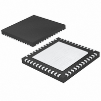
LTC2393CUK-16#TRPBF Linear Technology, LTC2393CUK-16#TRPBF Datasheet - Page 16

LTC2393CUK-16#TRPBF
Manufacturer Part Number
LTC2393CUK-16#TRPBF
Description
IC ADC 16BIT SER/PAR 1M 48-QFN
Manufacturer
Linear Technology
Datasheet
1.LTC2393ILX-16PBF.pdf
(24 pages)
Specifications of LTC2393CUK-16#TRPBF
Number Of Bits
16
Sampling Rate (per Second)
1M
Data Interface
Serial, Parallel
Number Of Converters
1
Power Dissipation (max)
175mW
Voltage Supply Source
Analog and Digital
Operating Temperature
0°C ~ 70°C
Mounting Type
Surface Mount
Package / Case
48-WFQFN, Exposed Pad
Lead Free Status / RoHS Status
Lead free / RoHS Compliant
Available stocks
Company
Part Number
Manufacturer
Quantity
Price
Part Number:
LTC2393CUK-16#TRPBFLTC2393CUK-16#PBF
Manufacturer:
Linear Technology
Quantity:
135
LTC2393-16
APPLICATIONS INFORMATION
Parallel Modes
The parallel output data interface is active when the
SER/PAR pin is tied low and when both CS and RD are low.
The output data can be read as a 16-bit word as shown
in Figures 8, 9 and 10 or it can be read as two 8-bit bytes
by using the BYTESWAP pin. As shown in Figure 11, with
the BYTESWAP pin low, the first eight MSBs are output on
the D15 to D8 pins and the eight LSBs are output on the
D7 to DO pins. When BYTESWAP is taken high, the eight
LSBs now are output on the D15 to D8 pins and the eight
MSBs are output on the D7 to D0 pins.
Serial Modes
The serial output data interface is active when the
SER/PAR pin is tied high and when both CS and RD are low.
The serial output data will be clocked out on the SDOUT
pin when an external clock is applied to the SCLK pin.
Clocking out the data after the conversion will yield the
best performance. With a shift clock frequency of at least
40MHz, a 1Msps throughput is still achieved. The serial
output data changes state on the rising edge of SCLK and
can be captured on the falling edge of SCLK. D15 remains
valid till the first rising edge of shift clock after the first
falling edge of shift clock. The non-active digital outputs
are high impedance when operating in the serial mode.
16
DATA BUS D[15:0]
CNVST
BUSY
Figure 8. Read the Parallel Data Continuously.
The Data Bus is Always Driven and Can’t Be Shared
CS = RD = 0
t
6
t
4
PREVIOUS CONVERSION
The SDIN input pin is used to daisy-chain multiple con-
verters. This is useful for applications where hardware
constraints may limit the number of lines needed to
interface to a large number of converters. For example,
if two devices are cascaded, the MSB of the first device
will appear at the output after 17 SCLK cycles. The first
MSB is clocked in on the falling edge of the first SCLK.
See Figure 12.
Data Format
When OB/2C is high, the digital output is offset binary.
When low, the MSB is inverted resulting in two’s comple-
ment output. This pin is active in both the parallel and
serial modes of operation.
Reset
When the RESET pin is high, the LTC2393-16 is reset, and
if this occurs during a conversion, the conversion is halted
and the data bus is put into Hi-Z mode. In reset, requests
for new conversions are ignored. Once RESET returns low,
the LTC2393-16 is ready to start a new conversion after
the acquisition time has been met. See Figure 13.
t
CONV
NEW
239316 F08
t
16
239316f


