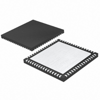
LTC2220CUP-1#TRPBF Linear Technology, LTC2220CUP-1#TRPBF Datasheet - Page 21

LTC2220CUP-1#TRPBF
Manufacturer Part Number
LTC2220CUP-1#TRPBF
Description
IC ADC 12BIT 185MSPS 64-QFN
Manufacturer
Linear Technology
Datasheet
1.LTC2220CUP-1TRPBF.pdf
(28 pages)
Specifications of LTC2220CUP-1#TRPBF
Number Of Bits
12
Sampling Rate (per Second)
185M
Data Interface
Parallel
Number Of Converters
1
Power Dissipation (max)
1.18W
Voltage Supply Source
Single Supply
Operating Temperature
0°C ~ 70°C
Mounting Type
Surface Mount
Package / Case
64-WFQFN, Exposed Pad
Lead Free Status / RoHS Status
Lead free / RoHS Compliant
Available stocks
Company
Part Number
Manufacturer
Quantity
Price
Output Driver Power
Separate output power and ground pins allow the output
drivers to be isolated from the analog circuitry. The power
supply for the digital output buffers, OV
to the same power supply as for the logic being driven. For
example if the converter is driving a DSP powered by a 1.8V
supply then OV
In the CMOS output mode, OV
voltage up to 3.6V. OGND can be powered with any voltage
from GND up to 1V and must be less than OV
outputs will swing between OGND and OV
In the LVDS output mode, OV
3.3V supply and OGND should be connected to GND.
Output Enable
The outputs may be disabled with the output enable pin, OE.
In CMOS or LVDS output modes OE high disables all data
outputs including OF and CLKOUT. The data access and bus
relinquish times are too slow to allow the outputs to be
enabled and disabled during full speed operation. The output
Hi-Z state is intended for use during long periods of
inactivity.
The Hi-Z state is not a truly open circuit; the output pins that
make an LVDS output pair have a 20k resistance between
them. Therefore in the CMOS output mode, adjacent data
bits will have 20k resistance in between them, even in the
Hi-Z state.
Sleep and Nap Modes
The converter may be placed in shutdown or nap modes
to conserve power. Connecting SHDN to GND results in
normal operation. Connecting SHDN to V
results in sleep mode, which powers down all circuitry
including the reference and typically dissipates 1mW. When
exiting sleep mode it will take milliseconds for the output
data to become valid because the reference capacitors have
to recharge and stabilize. Connecting SHDN to V
to GND results in nap mode, which typically dissipates
APPLICATIO S I FOR ATIO
DD
should be tied to that same 1.8V supply.
U
U
DD
DD
should be connected to a
can be powered with any
W
DD
DD
, should be tied
DD
and OE to V
DD
.
. The logic
U
DD
and OE
DD
35mW. In nap mode, the on-chip reference circuit is kept
on, so that recovery from nap mode is faster than that from
sleep mode, typically taking 100 clock cycles. In both sleep
and nap mode all digital outputs are disabled and enter the
Hi-Z state.
GROUNDING AND BYPASSING
The LTC2220-1 requires a printed circuit board with a clean
unbroken ground plane. A multilayer board with an inter-
nal ground plane is recommended. Layout for the printed
circuit board should ensure that digital and analog signal
lines are separated as much as possible. In particular, care
should be taken not to run any digital signal alongside an
analog signal or underneath the ADC.
High quality ceramic bypass capacitors should be used at
the V
as shown in the block diagram on the front page of this data
sheet. Bypass capacitors must be located as close to the
pins as possible. Of particular importance are the capaci-
tors between REFHA and REFLB and between REFHB and
REFLA. These capacitors should be as close to the device
as possible (1.5mm or less). Size 0402 ceramic capacitors
are recommended. The 2.2µF capacitor between REFHA and
REFLA can be somewhat further away. The traces connect-
ing the pins and bypass capacitors must be kept short and
should be made as wide as possible.
The LTC2220-1 differential inputs should run parallel and
close to each other. The input traces should be as short as
possible to minimize capacitance and to minimize noise
pickup.
HEAT TRANSFER
Most of the heat generated by the LTC2220-1 is transferred
from the die through the bottom-side exposed pad and
package leads onto the printed circuit board. For good
electrical and thermal performance, the exposed pad should
be soldered to a large grounded pad on the PC board. It is
critical that all ground pins are connected to a ground plane
of sufficient area.
DD
, OV
DD
, V
CM
, REFHA, REFHB, REFLA and REFLB pins
LTC2220-1
21
2220_1fa


