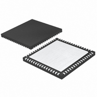
LTC2208CUP-14#TR Linear Technology, LTC2208CUP-14#TR Datasheet - Page 20

LTC2208CUP-14#TR
Manufacturer Part Number
LTC2208CUP-14#TR
Description
IC ADC 14BIT 130MSPS 64-QFN
Manufacturer
Linear Technology
Datasheet
1.LTC2208CUP-14TR.pdf
(28 pages)
Specifications of LTC2208CUP-14#TR
Number Of Bits
14
Sampling Rate (per Second)
130M
Data Interface
Parallel
Number Of Converters
1
Power Dissipation (max)
1.78W
Voltage Supply Source
Single Supply
Operating Temperature
0°C ~ 70°C
Mounting Type
Surface Mount
Package / Case
64-WFQFN, Exposed Pad
Lead Free Status / RoHS Status
Contains lead / RoHS non-compliant
LTC2208-14
APPLICATIONS INFORMATION
Figure 4a shows transformer coupling using a transmis-
sion line balun transformer. This type of transformer has
much better high frequency response and balance than
fl ux coupled center tap transformers. Coupling capaci-
tors are added at the ground and input primary terminals
to allow the secondary terminals to be biased at 1.25V.
Figure 4b shows the same circuit with components suit-
able for higher input frequencies.
Direct Coupled Circuits
Figure 5 demonstrates the use of a differential amplifi er to
convert a single ended input signal into a differential input
signal. The advantage of this method is that it provides
low frequency input response; however, the limited gain
bandwidth of any op amp or closed-loop amplifi er will de-
grade the ADC SFDR at high input frequencies. Additionally,
wideband op amps or differential amplifi ers tend to have
high noise. As a result, the SNR will be degraded unless
the noise bandwidth is limited prior to the ADC input.
20
ANALOG
ANALOG
Figure 4b. Using a Transmission Line Balun Transformer.
Recommended for Input Frequencies from 250MHz to 500MHz
Figure 4a. Using a Transmission Line Balun Transformer.
Recommended for Input Frequencies from 100MHz to 250MHz
INPUT
INPUT
0.1μF
0.1μF
0.1μF
0.1μF
T1 = MA/COM ETC1-1-13
RESISTORS, CAPACITORS
ARE 0402 PACKAGE SIZE
EXCEPT 2.2μF
T1 = MA/COM ETC1-1-13
RESISTORS, CAPACITORS
ARE 0402 PACKAGE SIZE
EXCEPT 2.2μF
1:1
1:1
T1
T1
25Ω
25Ω
25Ω
25Ω
0.1μF
0.1μF
10Ω
10Ω
4.7pF
4.7pF
2.2μF
2.2pF
2.2pF
5Ω
5Ω
2.2μF
5Ω
5Ω
4.7pF
V
A
A
V
A
A
CM
IN
IN
CM
IN
IN
+
–
+
–
LTC2208-14
LTC2208-14
220814 F04b
220814 F04a
Reference Operation
Figure 6 shows the LTC2208-14 reference circuitry con-
sisting of a 2.5V bandgap reference, a programmable gain
amplifi er and control circuit. The LTC2208-14 has three
modes of reference operation: Internal Reference, 1.25V
external reference or 2.5V external reference. To use the
internal reference, tie the SENSE pin to V
external reference, simply apply either a 1.25V or 2.5V
reference voltage to the SENSE input pin. Both 1.25V
and 2.5V applied to SENSE will result in a full scale range
of 2.25V
for a common mode bias for input drive circuitry. An
external bypass capacitor is required for the V
This provides a high frequency low impedance path to
ground for internal and external circuitry. This is also the
compensation capacitor for the reference; it will not be
stable without this capacitor. The minimum value required
for stability is 2.2μF .
TIE TO V
EXTERNAL 1.25V
EXTERNAL 2.5V
INTERNAL 2.5V
OR INPUT FOR
OR INPUT FOR
ANALOG
REFERENCE
Figure 5. DC Coupled Input with Differential Amplifi er
INPUT
REFERENCE
REFERENCE
DD
TO USE
P-P
AMPLIFIER = LTC6600-20,
LT1993, ETC.
(PGA = 0). A 1.25V output, V
SENSE
DIFFERENTIAL
CM
–
+
2.2μF
V
HIGH SPEED
AMPLIFIER
Figure 6. Reference Circuit
CM
+
–
BUFFER
25Ω
25Ω
AND GAIN
CONTROL
SELECT
RANGE
2.2μF
12pF
12pF
1.25V
V
A
A
CM
IN
IN
+
–
CM
DD
PGA
LTC2208-14
. To use an
is provided
CM
REFERENCE
BANDGAP
REFERENCE
220814 F05
INTERNAL
2.5V
output.
ADC
220814fb
220814 F06


