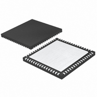
LTC2242IUP-10#PBF Linear Technology, LTC2242IUP-10#PBF Datasheet - Page 10

LTC2242IUP-10#PBF
Manufacturer Part Number
LTC2242IUP-10#PBF
Description
IC ADC 10BIT 250MSPS 64-QFN
Manufacturer
Linear Technology
Datasheet
1.LTC2242CUP-10PBF.pdf
(28 pages)
Specifications of LTC2242IUP-10#PBF
Number Of Bits
10
Sampling Rate (per Second)
250M
Data Interface
Parallel
Number Of Converters
1
Power Dissipation (max)
975mW
Voltage Supply Source
Single Supply
Operating Temperature
-40°C ~ 85°C
Mounting Type
Surface Mount
Package / Case
64-WFQFN, Exposed Pad
Lead Free Status / RoHS Status
Lead free / RoHS Compliant
LTC2242-10
PIN FUNCTIONS
AIN
AIN
REFHA (Pins 5, 6): ADC High Reference. Bypass to
Pins 7, 8 with 0.1μF ceramic chip capacitor, to Pins 11,
12 with a 2.2μF ceramic capacitor and to ground with 1μF
ceramic capacitor.
REFLB (Pins 7, 8): ADC Low Reference. Bypass to Pins
5, 6 with 0.1μF ceramic chip capacitor. Do not connect to
Pins 11, 12.
REFHB (Pins 9, 10): ADC High Reference. Bypass to
Pins 11, 12 with 0.1μF ceramic chip capacitor. Do not
connect to Pins 5, 6.
REFLA (Pins 11, 12): ADC Low Reference. Bypass to
Pins 9, 10 with 0.1μF ceramic chip capacitor, to Pins 5,
6 with a 2.2μF ceramic capacitor and to ground with 1μF
ceramic capacitor.
V
GND with 0.1μF ceramic chip capacitors.
GND (Pins 16, 61, 64): ADC Power Ground.
ENC
positive edge.
ENC
starts on the negative edge. Bypass to ground with 0.1μF
ceramic for single-ended encode signal.
SHDN (Pin 19): Shutdown Mode Selection Pin. Connecting
SHDN to GND and OE to GND results in normal operation
with the outputs enabled. Connecting SHDN to GND and
OE to V
high impedance. Connecting SHDN to V
results in nap mode with the outputs at high impedance.
Connecting SHDN to V
mode with the outputs at high impedance.
OE (Pin 20): Output Enable Pin. Refer to SHDN pin function.
DNC (Pins 21, 22, 23, 24): Do not connect these pins.
D0
38, 39, 40, 43, 44, 45, 46, 47, 48, 51, 52, 53, 54):
LVDS Digital Outputs. All LVDS outputs require differential
100Ω termination resistors at the LVDS receiver. D9
is the MSB.
10
DD
–
+
–
/D0
+
–
(Pins 13, 14, 15, 62, 63): 2.5V Supply. Bypass to
(Pins 1, 2): Positive Differential Analog Input.
(Pins 3, 4): Negative Differential Analog Input.
(Pin 17): Encode Input. Conversion starts on the
(Pin 18): Encode Complement Input. Conversion
DD
+
to D9
results in normal operation with the outputs at
–
/D9
+
(Pins 27, 28, 29, 30, 31, 32, 37,
DD
and OE to V
(LVDS Mode)
DD
DD
results in sleep
and OE to GND
–
/D9
+
OGND (Pins 25, 33, 41, 50): Output Driver Ground.
OV
put Drivers. Bypass to ground with 0.1μF ceramic chip
capacitor.
CLKOUT
Output. Latch data on rising edge of CLKOUT
edge of CLKOUT
OF
High when an over or under fl ow has occurred.
LVDS (Pin 57): Output Mode Selection Pin. Connecting
LVDS to 0V selects full rate CMOS mode. Connecting LVDS
to 1/3V
update. Connecting LVDS to 2/3V
mode with interleaved update. Connecting LVDS to V
selects LVDS mode.
MODE (Pin 58): Output Format and Clock Duty Cycle
Stabilizer Selection Pin. Connecting MODE to 0V selects
offset binary output format and turns the clock duty cycle
stabilizer off. Connecting MODE to 1/3V
binary output format and turns the clock duty cycle stabilizer
on. Connecting MODE to 2/3V
output format and turns the clock duty cycle stabilizer on.
Connecting MODE to V
format and turns the clock duty cycle stabilizer off.
SENSE (Pin 59): Reference Programming Pin. Connecting
SENSE to V
input range. Connecting SENSE to V
reference and a ±1V input range. An external reference
greater than 0.5V and less than 1V applied to SENSE
selects an input range of ±V
input range.
V
Bypass to ground with 2.2μF ceramic chip capacitor.
GND (Exposed Pad) (Pin 65): ADC Power Ground. The
exposed pad on the bottom of the package needs to be
soldered to ground.
CM
–
DD
/OF
(Pin 60): 1.25V Output and Input Common Mode Bias.
(Pins 26, 34, 42, 49): Positive Supply for the Out-
DD
+
–
(Pins 55 to 56): LVDS Over/Under Flow Output.
/CLKOUT
selects demux CMOS mode with simultaneous
CM
selects the internal reference and a ±0.5V
+
.
+
(Pins 35 to 36): LVDS Data Valid
DD
selects 2’s complement output
SENSE
DD
DD
selects 2’s complement
. ±1V is the largest valid
DD
selects demux CMOS
selects the internal
DD
selects offset
–
, falling
224210fc
DD


