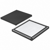
LTC2242IUP-10#PBF Linear Technology, LTC2242IUP-10#PBF Datasheet - Page 18

LTC2242IUP-10#PBF
Manufacturer Part Number
LTC2242IUP-10#PBF
Description
IC ADC 10BIT 250MSPS 64-QFN
Manufacturer
Linear Technology
Datasheet
1.LTC2242CUP-10PBF.pdf
(28 pages)
Specifications of LTC2242IUP-10#PBF
Number Of Bits
10
Sampling Rate (per Second)
250M
Data Interface
Parallel
Number Of Converters
1
Power Dissipation (max)
975mW
Voltage Supply Source
Single Supply
Operating Temperature
-40°C ~ 85°C
Mounting Type
Surface Mount
Package / Case
64-WFQFN, Exposed Pad
Lead Free Status / RoHS Status
Lead free / RoHS Compliant
APPLICATIONS INFORMATION
LTC2242-10
Other voltage ranges in between the pin selectable ranges
can be programmed with two external resistors as shown
in Figure 10. An external reference can be used by ap-
plying its output directly or through a resistor divider to
SENSE. It is not recommended to drive the SENSE pin
with a logic device. The SENSE pin should be tied to the
appropriate level as close to the converter as possible. If
18
TIE TO V
TIE TO V
RANGE = 2 • V
CM
0.5V < V
DD
FOR 2V RANGE;
FOR 1V RANGE;
SENSE
SENSE
Figure 9. Equivalent Reference Circuit
1.25V
1μF
1μF
< 1V
FOR
Figure 10. 1.5V Range ADC
0.75V
8k
12k
1.25V
2.2μF
0.1μF
2.2μF
0.1μF
SENSE
REFHA
REFHB
REFLB
REFLA
V
CM
SENSE
2.2μF
1μF
V
LTC2242-10
CM
CONTROL
DETECT
2Ω
RANGE
AND
LTC2242-10
1.25V BANDGAP
224210 F10
DIFF AMP
REFERENCE
INTERNAL ADC
HIGH REFERENCE
INTERNAL ADC
LOW REFERENCE
1V
BUFFER
0.5V
224210 F09
the SENSE pin is driven externally, it should be bypassed
to ground as close to the device as possible with a 1μF
ceramic capacitor.
Input Range
The input range can be set based on the application.
The 2V input range will provide the best signal-to-noise
performance while maintaining excellent SFDR. The 1V
input range will have better SFDR performance, but the
SNR will degrade by 1.7dB. See the Typical Performance
Characteristics section.
Driving the Encode Inputs
The noise performance of the LTC2242-10 can depend
on the encode signal quality as much as on the analog
input. The ENC
differentially, primarily for noise immunity from com-
mon mode noise sources. Each input is biased through
a 4.8k resistor to a 1.5V bias. The bias resistors set the
DC operating point for transformer coupled drive circuits
and can set the logic threshold for single-ended drive
circuits.
Any noise present on the encode signal will result in ad-
ditional aperture jitter that will be RMS summed with the
inherent ADC aperture jitter.
In applications where jitter is critical (high input frequen-
cies) take the following into consideration:
1. Differential drive should be used.
2. Use as large an amplitude as possible; if transformer
coupled use a higher turns ratio to increase the ampli-
tude.
3. If the ADC is clocked with a sinusoidal signal, fi lter the
encode signal to reduce wideband noise.
4. Balance the capacitance and series resistance at both
encode inputs so that any coupled noise will appear at both
inputs as common mode noise. The encode inputs have a
common mode range of 1.2V to 2.0V. Each input may be
driven from ground to V
+
/ENC
–
inputs are intended to be driven
DD
for single-ended drive.
224210fc


