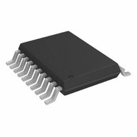
AD7997BRUZ-0 Analog Devices Inc, AD7997BRUZ-0 Datasheet - Page 10

AD7997BRUZ-0
Manufacturer Part Number
AD7997BRUZ-0
Description
IC ADC 10BIT 8CHAN I2C 20TSSOP
Manufacturer
Analog Devices Inc
Datasheet
1.AD7997BRUZ-1.pdf
(32 pages)
Specifications of AD7997BRUZ-0
Data Interface
I²C, Serial
Number Of Bits
10
Sampling Rate (per Second)
188k
Number Of Converters
1
Power Dissipation (max)
2.2mW
Voltage Supply Source
Single Supply
Operating Temperature
-40°C ~ 85°C
Mounting Type
Surface Mount
Package / Case
20-TSSOP (0.173", 4.40mm Width)
Resolution (bits)
10bit
Sampling Rate
188kSPS
Input Channel Type
Single Ended
Supply Voltage Range - Analog
2.7V To 5.5V
Supply Current
1.4mA
Number Of Elements
1
Resolution
10Bit
Architecture
SAR
Sample Rate
188KSPS
Input Polarity
Unipolar
Input Type
Voltage
Rated Input Volt
2.5V
Differential Input
No
Power Supply Requirement
Single
Single Supply Voltage (typ)
3.3/5V
Single Supply Voltage (min)
2.7V
Single Supply Voltage (max)
5.5V
Dual Supply Voltage (typ)
Not RequiredV
Dual Supply Voltage (min)
Not RequiredV
Dual Supply Voltage (max)
Not RequiredV
Power Dissipation
6.05mW
Differential Linearity Error
±0.5LSB
Integral Nonlinearity Error
±0.5LSB
Operating Temp Range
-40C to 85C
Operating Temperature Classification
Industrial
Mounting
Surface Mount
Pin Count
20
Package Type
TSSOP
Input Signal Type
Single-Ended
Lead Free Status / RoHS Status
Lead free / RoHS Compliant
For Use With
EVAL-AD7997CBZ - BOARD EVALUATION AD7997
Lead Free Status / Rohs Status
Compliant
Available stocks
Company
Part Number
Manufacturer
Quantity
Price
Part Number:
AD7997BRUZ-0
Manufacturer:
ADI/亚德诺
Quantity:
20 000
AD7997/AD7998
PIN CONFIGURATION AND PIN FUNCTION DESCRIPTIONS
Table 5. Pin Function Descriptions
Pin No.
1, 3,
4, 20
2, 5
6
7
8
9
10
11
12
13
14
15
16
17
18
19
Table 6. I
Part Number
AD7997-0
AD7997-0
AD7997-1
AD7997-1
AD7997-x
AD7998-0
AD7998-0
AD7998-1
AD7998-1
AD7998-x
1
If the AS pin is left floating on any of the AD7997/AD7998 parts, the device address is 010 0000.
1
1
2
C Address Selection
Mnemonic
AGND
V
REF
V
V
V
V
V
V
V
V
AS
CONVST
ALERT/BUSY
SDA
SCL
DD
IN
IN
IN
IN
IN
IN
IN
IN
1
3
5
7
8
6
4
2
IN
Function
Analog Ground. Ground reference point for all circuitry on the AD7997/AD7998. All analog input signals should be
referred to this AGND voltage.
Power Supply Input. The V
Voltage Reference Input. The external reference for the AD7997/AD7998 should be applied to this input pin. The
voltage range for the external reference is 1.2 V to V
and AGND. See Typical Connection Diagram.
Analog Input 1. Single-ended analog input channel. The input range is 0 V to REF
Analog Input 3. Single-ended analog input channel. The input range is 0 V to REF
Analog Input 5. Single-ended analog input channel. The input range is 0 V to REF
Analog Input 7. Single-ended analog input channel. The input range is 0 V to REF
Analog Input 8. Single-ended analog input channel. The input range is 0 V to REF
Analog Input 6. Single-ended analog input channel. The input range is 0 V to REF
Analog Input 4. Single-ended analog input channel. The input range is 0 V to REF
Analog Input 2. Single-ended analog input channel. The input range is 0 V to REF
Logic Input. Address select input that selects one of three I
The device address depends on the voltage applied to this pin.
Logic Input Signal. Convert start signal. This is an edge-triggered logic input. The rising edge of this signal powers up
the part. The power-up time for the part is 1 µs. The falling edge of CONVST places the track/hold into hold mode and
initiates a conversion. A power-up time of at least 1 µs must be allowed for the CONVST high pulse; otherwise, the
conversion result is invalid (see the Modes of Operation section).
Digital Output. Selectable as an ALERT or BUSY output function. When configured as an ALERT, this pin acts as an out-
of-range indicator and, if enabled, becomes active when the conversion result violates the DATAHIGH or DATALOW
register values. See the Limit Registers section. When configured as a BUSY output, this pin becomes active when a
conversion is in progress. Open-drain output.
Digital I/O. Serial bus bidirectional data. Open-drain output. External pull-up resistor required.
Digital Input. Serial bus clock. Open-drain input. External pull-up resistor required.
AS Pin
AGND
V
AGND
V
Float
AGND
V
AGND
V
Float
DD
DD
DD
DD
Figure 3. AD7998/AD7997 Pin Configuration
AGND
AGND
AGND
REF
DD
V
V
V
V
V
V
IN
IN
IN
IN
DD
DD
IN
range for the AD7997/AD7998 is from 2.7 V to 5.5 V.
1
3
5
7
10
1
2
3
4
5
6
7
8
9
(Not to Scale)
Rev. 0 | Page 10 of 32
AD7997/
AD7998
TOP VIEW
20
19
18
17
16
15
14
13
12
11
CONVST
AGND
SCL
SDA
ALERT/BUSY
AS
V
V
V
V
IN
IN
IN
IN
DD
2
4
6
8
. A 0.1 µF and 1 µF capacitors should be placed between REF
I
010 0001
010 0010
010 0011
010 0100
010 0000
010 0001
010 0010
010 0011
010 0100
010 0000
2
C Address
2
C addresses for the AD7997/AD7998, as shown in Table
IN
IN
IN
IN
IN
IN
IN
IN
.
.
.
.
.
.
.
.
IN
6
.


