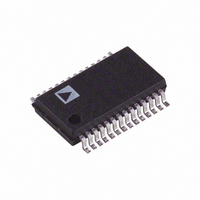
AD9280ARS Analog Devices Inc, AD9280ARS Datasheet - Page 15

AD9280ARS
Manufacturer Part Number
AD9280ARS
Description
IC ADC CMOS 8BIT 32MSPS 28-SSOP
Manufacturer
Analog Devices Inc
Datasheet
1.AD9280ARSZ.pdf
(24 pages)
Specifications of AD9280ARS
Rohs Status
RoHS non-compliant
Number Of Bits
8
Sampling Rate (per Second)
32M
Data Interface
Parallel
Number Of Converters
9
Power Dissipation (max)
110mW
Voltage Supply Source
Single Supply
Operating Temperature
-40°C ~ 85°C
Mounting Type
Surface Mount
Package / Case
28-SSOP (0.200", 5.30mm Width)
Number Of Elements
1
Resolution
8Bit
Architecture
Pipelined
Sample Rate
32MSPS
Input Polarity
Unipolar
Input Type
Voltage
Rated Input Volt
3V
Differential Input
Yes
Power Supply Requirement
Analog and Digital
Single Supply Voltage (typ)
3V
Single Supply Voltage (min)
2.7V
Single Supply Voltage (max)
5.5V
Dual Supply Voltage (typ)
Not RequiredV
Dual Supply Voltage (min)
Not RequiredV
Dual Supply Voltage (max)
Not RequiredV
Power Dissipation
110mW
Differential Linearity Error
±1LSB
Integral Nonlinearity Error
±1.5LSB
Operating Temp Range
-40C to 85C
Operating Temperature Classification
Industrial
Mounting
Surface Mount
Pin Count
28
Package Type
SSOP
For Use With
AD9280-EB - BOARD EVAL FOR AD9280
Lead Free Status / RoHS Status
Not Compliant
Available stocks
Company
Part Number
Manufacturer
Quantity
Price
Company:
Part Number:
AD9280ARS
Manufacturer:
PANASONIC
Quantity:
2 600
Part Number:
AD9280ARS
Manufacturer:
ADI/亚德诺
Quantity:
20 000
Part Number:
AD9280ARSZ
Manufacturer:
ADI/亚德诺
Quantity:
20 000
Part Number:
AD9280ARSZRL
Manufacturer:
ADI/亚德诺
Quantity:
20 000
DIFFERENTIAL INPUT OPERATION
The AD9280 will accept differential input signals. This function
may be used by shorting REFTS and REFBS and driving them
as one leg of the differential signal (the top leg is driven into
AIN). In the configuration below, the AD9280 is accepting a
1 V p-p signal. See Figure 29.
AD876-8 MODE OF OPERATION
The AD9280 may be dropped into the AD876-8 socket. This
will allow AD876-8 users to take advantage of the reduced
power consumption realized when running the AD9280 on a
3.0 V analog supply.
Figure 30 shows the pin functions of the AD876-8 and AD9280.
The grounded REFSENSE pin and floating MODE pin effec-
tively put the AD9280 in the external reference mode. The
external reference input for the AD876-8 will now be placed
on the reference pins of the AD9280.
The clamp controls will be grounded by the AD876-8 socket.
The AD9280 has a 3 clock cycle delay compared to a 3.5 cycle
delay of the AD876-8.
CLOCK INPUT
The AD9280 clock input is buffered internally with an inverter
powered from the AVDD pin. This feature allows the AD9280
to accommodate either +5 V or +3.3 V CMOS logic input sig-
nal swings with the input threshold for the CLK pin nominally
at AVDD/2.
REV. E
2V
1V
4V
2V
4V
2V
1.0 F
Figure 29. Differential Input
0.1 F
0.1 F
Figure 30. AD876 Mode
AVDD/2
10 F
AVDD/2
AVDD
0.1 F
0.1 F
REFTS
REFBS
AIN
VREF
REFSENSE
MODE
AD9280
NC
REFTF
REFBF
AIN
REFTS
REFTF
REFBF
REFBS
MODE
REFSENSE
CLAMP
CLAMPIN
OTR
AD9280
VREF
0.1 F
0.1 F
10 F
0.1 F
0.1 F
–15–
The pipelined architecture of the AD9280 operates on both
rising and falling edges of the input clock. To minimize duty
cycle variations the recommended logic family to drive the clock
input is high speed or advanced CMOS (HC/HCT, AC/ACT)
logic. CMOS logic provides both symmetrical voltage threshold
levels and sufficient rise and fall times to support 32 MSPS
operation. The AD9280 is designed to support a conversion rate
of 32 MSPS; running the part at slightly faster clock rates may
be possible, although at reduced performance levels. Conversely,
some slight performance improvements might be realized by
clocking the AD9280 at slower clock rates.
The power dissipated by the output buffers is largely propor-
tional to the clock frequency; running at reduced clock rates
provides a reduction in power consumption.
DIGITAL INPUTS AND OUTPUTS
Each of the AD9280 digital control inputs, THREE-STATE
and STBY are reference to analog ground. The clock is also
referenced to analog ground.
The format of the digital output is straight binary (see Figure
32). A low power mode feature is provided such that for STBY
= HIGH and the clock disabled, the static power of the AD9280
will drop below 5 mW.
THREE-
(D0–D9)
STATE
ANALOG
OUTPUT
DATA
CLOCK
INPUT
INPUT
DATA
Figure 33. Three-State Timing Diagram
S1
Figure 32. Output Data Format
OTR
t
Figure 31. Timing Diagram
CH
t
C
–FS
t
CL
–FS+1LSB
t
DHZ
S2
IMPEDANCE
HIGH
S3
+FS–1LSB
+FS
t
DEN
AD9280
S4
DATA 1
25ns


