AD7476AAKSZ-500RL7 Analog Devices Inc, AD7476AAKSZ-500RL7 Datasheet - Page 11
AD7476AAKSZ-500RL7
Manufacturer Part Number
AD7476AAKSZ-500RL7
Description
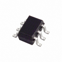
IC ADC 12BIT 1MSPS LP SC70-6
Manufacturer
Analog Devices Inc
Datasheet
1.AD7477AARMZ.pdf
(28 pages)
Specifications of AD7476AAKSZ-500RL7
Resolution (bits)
12bit
Sampling Rate
1MSPS
Input Channel Type
Single Ended
Data Interface
Serial, SPI
Supply Current
3.5mA
Digital Ic Case Style
SC-70
No. Of Pins
6
Lead Free Status / RoHS Status
Lead free / RoHS Compliant
Available stocks
Company
Part Number
Manufacturer
Quantity
Price

Part Number:
AD7476AAKSZ-500RL7
Manufacturer:
ADI/亚德诺
Quantity:
20 000


PIN CONFIGURATIONS AND FUNCTION DESCRIPTIONS
Table 6. Pin Function Descriptions
Mnemonic
CS
V
GND
V
SDATA
SCLK
NC
DD
IN
AD7476A/AD7477A/AD7478A and also frames the serial data transfer.
of four leading zeros followed by 10 bits of conversion data followed by two trailing zeros, provided MSB first. The data stream
from the AD7478A consists of four leading zeros followed by 8 bits of conversion data followed by four trailing zeros that are
provided MSB first.
Description
Chip Select. Active low logic input. This input provides the dual function of initiating conversions on the
Power Supply Input. The V
Analog Ground. Ground reference point for all circuitry on AD7476A/AD7477A/AD7478A. Refer all analog input signals to this
GND voltage.
Analog Input. Single-ended analog input channel. The input range is 0 V to V
Data Out. Logic output. The conversion result from AD7476A/AD7477A/AD7478A is provided on this output as a serial data
stream. The bits are clocked out on the falling edge of the SCLK input. The data stream from the AD7476A consists of four
leading zeros followed by 12 bits of conversion data that are provided MSB first. The data stream from the AD7477A consists
Serial Clock. Logic input. SCLK provides the serial clock for accessing data from the part. This clock input is also used as the
clock source for the conversion process of AD7476A/AD7477A/AD7478A.
No Connect.
Figure 5. 6-Lead SC70 Pin Configuration
GND
V
V
DD
IN
1
2
3
(Not to Scale)
AD7476A/
AD7477A/
AD7478A
TOP VIEW
6
5
4
CS
SDATA
SCLK
DD
range for AD7476A/AD7477A/AD7478A is from 2.35 V to 5.25 V.
Rev. F | Page 11 of 28
Figure 6. 8-Lead MSOP Pin Configuration
DD
.
SDATA
AD7476A/AD7477A/AD7478A
V
CS
NC
DD
NC = NO CONNECT
1
2
3
4
(Not to Scale)
AD7476A/
AD7477A/
AD7478A
TOP VIEW
8
7
6
5
V
GND
SCLK
NC
IN
Related parts for AD7476AAKSZ-500RL7
Image
Part Number
Description
Manufacturer
Datasheet
Request
R

Part Number:
Description:
12-Bit Low Power ADC In SC70 Package I.C
Manufacturer:
Analog Devices Inc
Datasheet:
Part Number:
Description:
12-Bit Low Power ADC In SC70 Package
Manufacturer:
Analog Devices Inc
Datasheet:
Part Number:
Description:
IC ADC 12BIT 1MSPS SC70-6 T/R
Manufacturer:
Analog Devices Inc
Datasheet:
Part Number:
Description:
IC ADC 12BIT 1MSPS SC70-6 T/R
Manufacturer:
Analog Devices Inc
Datasheet:

Part Number:
Description:
±1.7g Dual-Axis IMEMS Accelerometer Evaluation Board
Manufacturer:
Analog Devices Inc
Datasheet:

Part Number:
Description:
Inertial Sensor Evaluation System
Manufacturer:
Analog Devices Inc
Datasheet:
Part Number:
Description:
Manufacturer:
Analog Devices Inc
Datasheet:
Part Number:
Description:
Manufacturer:
Analog Devices Inc
Datasheet:
Part Number:
Description:
Manufacturer:
Analog Devices Inc
Datasheet:
Part Number:
Description:
Manufacturer:
Analog Devices Inc
Datasheet:
Part Number:
Description:
Manufacturer:
Analog Devices Inc
Datasheet:
Part Number:
Description:
Manufacturer:
Analog Devices Inc
Datasheet:
Part Number:
Description:
Manufacturer:
Analog Devices Inc
Datasheet: