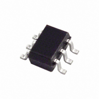
AD7476AAKSZ-500RL7 Analog Devices Inc, AD7476AAKSZ-500RL7 Datasheet - Page 23

AD7476AAKSZ-500RL7
Manufacturer Part Number
AD7476AAKSZ-500RL7
Description
IC ADC 12BIT 1MSPS LP SC70-6
Manufacturer
Analog Devices Inc
Datasheet
1.AD7477AARMZ.pdf
(28 pages)
Specifications of AD7476AAKSZ-500RL7
Resolution (bits)
12bit
Sampling Rate
1MSPS
Input Channel Type
Single Ended
Data Interface
Serial, SPI
Supply Current
3.5mA
Digital Ic Case Style
SC-70
No. Of Pins
6
Lead Free Status / RoHS Status
Lead free / RoHS Compliant
Available stocks
Company
Part Number
Manufacturer
Quantity
Price
Part Number:
AD7476AAKSZ-500RL7
Manufacturer:
ADI/亚德诺
Quantity:
20 000
MICROPROCESSOR INTERFACING
The serial interface on the AD7476A/AD7477A/AD7478A
allows the part to be directly connected to a range of different
microprocessors. This section explains how to interface the
AD7476A/AD7477A/AD7478A with some of the more
common microcontroller and DSP serial interface protocols.
AD7476A/AD7477A/AD7478A TO TMS320C541
INTERFACE
The serial interface on the TMS320C541 uses a continuous
serial clock and frame synchronization signals to synchronize
the data transfer operations with peripheral devices, such as
the AD7476A/AD7477A/AD7478A. The CS input allows easy
interfacing between the TMS320C541 and the AD7476A/
AD7477A/AD7478A without any glue logic required. The serial
port of the TMS320C541 is set up to operate in burst mode
(FSM = 1 in the serial port control register, SPC) with Internal
Serial Clock CLKX (MCM = 1 in the SPC register) and internal
frame signal (TXM = 1 in the SPC register), so both pins are
configured as outputs. For the AD7476A, set the word length to
16 bits (FO = 0 in the SPC register). This DSP only allows
frames with a word length of 16 bits or 8 bits. Therefore, in the
case of the AD7477A and AD7478A where 14 bits and 12 bits
are required, the FO bit is set up to 16 bits. This means that to
obtain the conversion result, 16 SCLKs are needed. In both
situations, the remaining SCLKs clock out trailing zeros. For the
AD7477A, two trailing zeros are clocked out in the last two clock
cycles; for the AD7478A, four trailing zeros are clocked out.
To summarize, the values in the SPC register are
FO = 0
FSM = 1
MCM = 1
TXM = 1
The format bit, FO, can be set to 1 to set the word length to
eight bits in order to implement the power-down mode on the
AD7476A/AD7477A/AD7478A.
Rev. F | Page 23 of 28
The connection diagram is shown in Figure 28. For signal
processing applications, it is imperative that the frame
synchronization signal from the TMS320C541 provide
equidistant sampling.
AD7476A/AD7477A/AD7478A TO ADSP-218x
INTERFACE
The ADSP-218x family of DSPs are interfaced directly to the
AD7476A/AD7477A/AD7478A without any glue logic
required. Set up the SPORT control register as follows:
TFSW = RFSW = 1, alternate framing
INVRFS = INVTFS = 1, active low frame signal
DTYPE = 00, right justify data
ISCLK = 1, internal serial clock
TFSR = RFSR = 1, frame every word
IRFS = 0, sets up RFS as an input
ITFS = 1, sets up TFS as an output
SLEN = 1111, 16 bits for the AD7476A
SLEN = 1101, 14 bits for the AD7477A
SLEN = 1011, 12 bits for the AD7478A
AD7476A/
AD7477A/
AD7478A
1
1
Figure 28. Interfacing to the TMS320C541
ADDITIONAL PINS OMITTED FOR CLARITY.
SDATA
SCLK
AD7476A/AD7477A/AD7478A
CS
CLKX
CLKR
DR
FSX
FSR
TMS320C541
1


