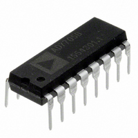
AD7705BNZ Analog Devices Inc, AD7705BNZ Datasheet - Page 35

AD7705BNZ
Manufacturer Part Number
AD7705BNZ
Description
IC ADC 16BIT 2CH 16-DIP
Manufacturer
Analog Devices Inc
Datasheet
1.AD7705BRUZ.pdf
(44 pages)
Specifications of AD7705BNZ
Data Interface
DSP, MICROWIRE™, QSPI™, Serial, SPI™
Number Of Bits
16
Sampling Rate (per Second)
500
Number Of Converters
1
Power Dissipation (max)
1mW
Voltage Supply Source
Single Supply
Operating Temperature
-40°C ~ 85°C
Mounting Type
Through Hole
Package / Case
16-DIP (0.300", 7.62mm)
Resolution (bits)
16bit
Sampling Rate
500SPS
Input Channel Type
Differential
Supply Current
1.3mA
Digital Ic Case Style
DIP
No. Of Pins
16
Lead Free Status / RoHS Status
Lead free / RoHS Compliant
For Use With
EVAL-AD7705EBZ - BOARD EVALUATION FOR AD7705
Lead Free Status / RoHS Status
Lead free / RoHS Compliant, Lead free / RoHS Compliant
Available stocks
Company
Part Number
Manufacturer
Quantity
Price
Part Number:
AD7705BNZ
Manufacturer:
ADI/亚德诺
Quantity:
20 000
AD7705/AD7706-to-8051 Interface
An interface circuit between the AD7705/AD7706 and the 8XC51
microcontroller is shown in Figure 23. The diagram shows the
minimum number of interface connections with CS on the
AD7705/AD7706 hardwired low. In the case of the 8XC51
interface, the minimum number of interconnects is two. In this
scheme, the DRDY bit of the communication register is monitored
to determine when the data register is updated. The alternative
scheme, which increases the number of interface lines to three,
is to monitor the DRDY output line from the AD7705/AD7706.
Monitoring the DRDY line can be done in two ways. First, DRDY
can be connected to a 8XC51 port bit (such as P1.0) that is
configured as an input. This port bit is then polled to determine
the status of DRDY . The second scheme is to use an interrupt-
driven system, in which case the DRDY output is connected to
the INT1 input of the 8XC51. For interfaces that require control
of the CS input on the AD7705/AD7706, a port bit of the 8XC51
(such as P1.1) that is configured as an output can be used to
drive the CS input. The 8XC51 is configured in Mode 0 serial
interface mode. Its serial interface contains a single data line.
As a result, the DOUT and DIN pins of the AD7705/
AD7706 should be connected together with a 10 kΩ pull-up
resistor. The serial clock on the 8XC51 idles high between data
transfers. During a write operation, the 8XC51 outputs the LSB
first. Because the AD7705/AD7706 expect the MSB first, the
data must be rearranged before being written to the output
serial register. Similarly, during a read operation, the AD7705/
AD7706 output the MSB first, and the 8XC51 expects the LSB
first. Therefore, the data read into the serial buffer must be
rearranged before the correct data-word from the AD7705/
AD7706 is available in the accumulator.
Figure 24. AD7705/AD7706-to-ADSP-2103/ADSP-2105 Interface
ADSP-2103/
ADSP-2105
SCLK
RFS
TFS
DR
DT
V
DD
AD7705/AD7706
RESET
DIN
CS
DOUT
SCLK
Rev. C | Page 35 of 44
AD7705/AD7706-to-ADSP-2103/ADSP-2105 Interface
Figure 24 shows an interface between the AD7705/AD7706 and
the ADSP-2103/ADSP-2105 DSP processor. In the interface
shown, the DRDY bit of the communication register is monitored
to determine when the data register is updated. The alternative
scheme is to use an interrupt-driven system, in which case the
DRDY output is connected to the IRQ2 input of the ADSP-2103/
ADSP-2105. The serial interface of the ADSP-2103/ADSP-2105
is set up for alternate framing mode. The RFS and TFS pins of
the ADSP-2103/ADSP-2105 are configured as active low outputs,
and the ADSP-2103/ADSP-2105 serial clock line, SCLK, is
configured as an output. The CS for the AD7705/AD7706 is
active when either the RFS or TFS outputs from the ADSP-2103/
ADSP-2105 are active. The serial clock rate on the ADSP-2103/
ADSP-2105 should be limited to 3 MHz to ensure correct
operation with the AD7705/AD7706.
CODE FOR SETTING UP THE AD7705/AD7706
The following section shows a set of read and write routines in
C code for interfacing the 68HC11 microcontroller to the AD7705.
The sample program sets up the various registers on the AD7705
and reads 1000 samples from one channel into the 68HC11. The
setup conditions on the part are the same as those outlined for the
flowchart of Figure 21. In the example code given here, the DRDY
output is polled to determine if a new valid word is available in
the data register. The same sequence is applicable for the AD7706.
The sequence of events in this program are as follows:
1.
2.
3.
4.
5.
6.
7.
Write to the communication register, selecting Channel 1
as the active channel and setting the next operation to be a
write to the clock register.
Write to the clock register, setting the CLKDIV bit, which
divides the external clock internally by two. This assumes
that the external crystal is 4.9512 MHz. The update rate is
selected to be 50 Hz.
Write to the communication register selecting Channel 1 as
the active channel and setting the next operation to be a
write to the setup register.
Write to the setup register, setting the gain to 1, setting
bipolar mode, buffer off, clearing the filter
synchronization, and initiating a self-calibration.
Poll the DRDY output.
Read the data from the data register.
Repeat Steps 5 and 6 (loop) until the specified number of
samples has been taken from the selected channel.
AD7705/AD7706


