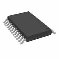
AD7714YRU Analog Devices Inc, AD7714YRU Datasheet - Page 9

AD7714YRU
Manufacturer Part Number
AD7714YRU
Description
IC ADC SIGNAL COND 3/5V 24-TSSOP
Manufacturer
Analog Devices Inc
Datasheet
1.AD7714YNZ.pdf
(40 pages)
Specifications of AD7714YRU
Rohs Status
RoHS non-compliant
Number Of Bits
24
Sampling Rate (per Second)
1k
Data Interface
DSP, MICROWIRE™, QSPI™, Serial, SPI™
Number Of Converters
1
Power Dissipation (max)
7mW
Voltage Supply Source
Analog and Digital
Operating Temperature
-40°C ~ 105°C
Mounting Type
Surface Mount
Package / Case
24-TSSOP (0.173", 4.40mm Width)
Number Of Elements
1
Resolution
24Bit
Architecture
Delta-Sigma
Sample Rate
1KSPS
Input Polarity
Unipolar/Bipolar
Input Type
Voltage
Differential Input
Yes
Power Supply Requirement
Analog and Digital
Single Supply Voltage (typ)
3/5V
Single Supply Voltage (min)
2.7V
Single Supply Voltage (max)
5.25V
Dual Supply Voltage (typ)
Not RequiredV
Dual Supply Voltage (min)
Not RequiredV
Dual Supply Voltage (max)
Not RequiredV
Power Dissipation
4.75mW
Integral Nonlinearity Error
±0.0015%FSR
Operating Temp Range
-40C to 105C
Operating Temperature Classification
Industrial
Mounting
Surface Mount
Pin Count
24
Package Type
TSSOP
For Use With
EVAL-AD7714-3EBZ - BOARD EVALUATION FOR AD7714
Lead Free Status / Rohs Status
Not Compliant
Available stocks
Company
Part Number
Manufacturer
Quantity
Price
Part Number:
AD7714YRUZ
Manufacturer:
ADI/亚德诺
Quantity:
20 000
DIP/SOIC PIN NUMBERS
Pin
No. Mnemonic
1
2
3
4
5
6
7
8
9
10
11
12
13
14
15
16
17
18
REV. C
SCLK
MCLK IN
MCLK OUT When the master clock for the device is a crystal/resonator, the crystal/resonator is connected between MCLK
POL
SYNC
RESET
AIN1
AIN2
AIN3
AIN4
STANDBY
AV
BUFFER
REF IN(–)
REF IN(+)
AIN5
AIN6
AGND
DD
Function
Serial Clock. Logic Input. An external serial clock is applied to this input to access serial data from the
AD7714. This serial clock can be a continuous clock with all data transmitted in a continuous train of pulses.
Alternatively, it can be a noncontinuous clock with the information being transmitted to the AD7714 in smaller
batches of data.
Master Clock signal for the device. This can be provided in the form of a crystal/resonator or external clock. A
crystal/resonator can be tied across the MCLK IN and MCLK OUT pins. Alternatively, the MCLK IN pin can
be driven with a CMOS-compatible clock and MCLK OUT left unconnected. The part is specified with clock
input frequencies of both 1 MHz and 2.4576 MHz.
IN and MCLK OUT. If an external clock is applied to the MCLK IN, MCLK OUT provides an inverted clock
signal. This clock can be used to provide a clock source for external circuits.
Clock Polarity. Logic Input. With this input low, the first transition of the serial clock in a data transfer
operation is from a low to a high. In microcontroller applications, this means that the serial clock should idle
low between data transfers. With this input high, the first transition of the serial clock in a data transfer
operation is from a high to a low. In microcontroller applications, this means that the serial clock should idle
high between data transfers.
Logic Input which allows for synchronization of the digital filters and analog modulators when using a number
of AD7714s. While SYNC is low, the nodes of the digital filter, the filter control logic and the calibration
control logic are reset and the analog modulator is also held in its reset state. SYNC does not affect the digital
interface and does not reset DRDY if it is low.
Logic Input. Active low input which resets the control logic, interface logic, digital filter and analog modulator
of the part to power-on status.
Analog Input Channel 1. Programmable-gain analog input which can be used as a pseudo-differential input
when used with AIN6 or as the positive input of a differential analog input pair when used with AIN2 (see
Communications Register section).
Analog Input Channel 2. Programmable-gain analog input which can be used as a pseudo-differential input
when used with AIN6 or as the negative input of a differential analog input pair when used with AIN1 (see
Communications Register section).
Analog Input Channel 3. Programmable-gain analog input which can be used as a pseudo-differential input
when used with AIN6 or as the positive input of a differential analog input pair when used with AIN4 (see
Communications Register section).
Analog Input Channel 4. Programmable-gain analog input which can be used as a pseudo-differential input
when used with AIN6 or as the negative input of a differential analog input pair when used with AIN3 (see
Communications Register section).
Logic Input. Taking this pin low shuts down the analog and digital circuitry, reducing current consumption to
typically 5 A.
Analog Positive Supply Voltage, A Grade Versions: +3.3 V nominal (AD7714-3) or +5 V nominal (AD7714-5);
Y Grade Versions: 3 V or 5 V nominal.
Buffer Option Select. Logic Input. With this input low, the on-chip buffer on the analog input (after the
multiplexer and before the analog modulator) is shorted out. With the buffer shorted out the current flowing in
the AV
allowing the inputs to handle higher source impedances.
Reference Input. Negative input of the differential reference input to the AD7714. The REF IN(–) can lie
anywhere between AV
Reference Input. Positive input of the differential reference input to the AD7714. The reference input is
differential with the provision that REF IN(+) must be greater than REF IN(–). REF IN(+) can lie anywhere
between AV
Analog Input Channel 5. Programmable-gain analog input which is the positive input of a differential analog
input pair when used with AIN6 (see Communications Register section).
Analog Input Channel 6. Reference point for AIN1 through AIN4 in pseudo-differential mode or as the
negative input of a differential input pair when used with AIN5 (see Communications Register section).
Ground reference point for analog circuitry.
DD
line is reduced to 270 A. With this input high, the on-chip buffer is in series with the analog input
DD
and AGND.
DD
and AGND provided REF IN(+) is greater than REF IN(–).
PIN FUNCTION DESCRIPTION
–9–
AD7714
2


