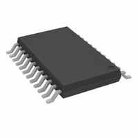
AD7730BRUZ Analog Devices Inc, AD7730BRUZ Datasheet - Page 3

AD7730BRUZ
Manufacturer Part Number
AD7730BRUZ
Description
IC ADC TRANSDUCER BRIDGE 24TSSOP
Manufacturer
Analog Devices Inc
Datasheet
1.AD7730LBRUZ.pdf
(52 pages)
Specifications of AD7730BRUZ
Data Interface
DSP, Serial, SPI™
Number Of Bits
24
Sampling Rate (per Second)
1.2k
Number Of Converters
1
Power Dissipation (max)
125mW
Voltage Supply Source
Analog and Digital
Operating Temperature
-40°C ~ 85°C
Mounting Type
Surface Mount
Package / Case
24-TSSOP (0.173", 4.40mm Width)
Resolution (bits)
24bit
Input Channel Type
Differential, Single Ended
Supply Voltage Range - Analog
4.75V To 5.25V
Supply Voltage Range - Digital
2.7V To 5.25V
Number Of Elements
1
Resolution
24Bit
Architecture
Delta-Sigma
Sample Rate
1.2KSPS
Input Polarity
Unipolar/Bipolar
Input Type
Voltage
Differential Input
Yes
Power Supply Requirement
Analog and Digital
Single Supply Voltage (typ)
5V
Single Supply Voltage (min)
4.75V
Single Supply Voltage (max)
5.25V
Dual Supply Voltage (typ)
Not RequiredV
Dual Supply Voltage (min)
Not RequiredV
Dual Supply Voltage (max)
Not RequiredV
Power Dissipation
125mW
Integral Nonlinearity Error
18ppm of FSR
Operating Temp Range
-40C to 85C
Operating Temperature Classification
Industrial
Mounting
Surface Mount
Pin Count
24
Package Type
TSSOP
Input Signal Type
Differential
Lead Free Status / RoHS Status
Lead free / RoHS Compliant
For Use With
EVAL-AD7730LEBZ - BOARD EVALUATION FOR AD7730EVAL-AD7730EBZ - BOARD EVAL FOR AD7730
Lead Free Status / Rohs Status
Compliant
Available stocks
Company
Part Number
Manufacturer
Quantity
Price
Company:
Part Number:
AD7730BRUZ
Manufacturer:
ADI
Quantity:
1 000
Part Number:
AD7730BRUZ
Manufacturer:
ADI/亚德诺
Quantity:
20 000
Part Number:
AD7730BRUZ-REEL
Manufacturer:
ADI/亚德诺
Quantity:
20 000
Company:
Part Number:
AD7730BRUZ-REEL7
Manufacturer:
ADI
Quantity:
1 000
REV. A
Parameter
LOGIC INPUTS
LOGIC OUTPUTS (Including MCLK OUT)
TRANSDUCER BURNOUT
OFFSET (TARE) DAC
SYSTEM CALIBRATION
POWER REQUIREMENTS
Input Current
All Inputs Except SCLK and MCLK IN
SCLK Only (Schmitt Triggered Input)
MCLK IN Only
V
V
V
V
Floating State Leakage Current
Floating State Output Capacitance
AIN1(+) Current
AIN1(–) Current
Initial Tolerance @ 25 C
Drift
Resolution
LSB Size
DAC Drift
DAC Drift vs. Time
Differential Linearity
Positive Full-Scale Calibration Limit
Negative Full-Scale Calibration Limit
Offset Calibration Limit
Input Span
Power Supply Voltages
Power Supply Currents
Power Dissipation
OL
OL
OH
OH
V
V
V
V
V
V
V
V
V
V
V
V
V
AV
DV
AV
AV
DV
DV
AV
Normal Mode
Standby Mode
, Output Low Voltage
, Output Low Voltage
INL
INL
INH
T+
T+
T–
T–
T+
T+
INL
INL
INH
INH
, Output High Voltage
, Output High Voltage
2
DD
DD
DD
DD
DD
DD
DD
, Input Low Voltage
, Input Low Voltage
– V
– V
, Input Low Voltage
, Input Low Voltage
, Input High Voltage
, Input High Voltage
, Input High Voltage
– AGND Voltage
Current (Normal Mode)
Current (Normal Mode)
+ DV
Voltage
Current (Normal Mode)
Current (Normal Mode)
T–
T–
16
17
DD
Current (Standby Mode)
4, 16
18
2
17
17
B Version
0.8
0.4
2.0
1.4/3
1/2.5
0.8/1.4
0.4/1.1
0.4/0.8
0.4/0.8
0.8
0.4
3.5
2.5
0.4
0.4
4.0
V
6
–100
100
0.1
6
2.3/2.6
2.5
25
–0.25/+0.75
1.05
–1.05
–1.05
0.8 FS
2.1 FS
+4.75 to +5.25
+2.7 to +5.25
10.3
22.3
1.3
2.7
25
65
125
125
10
10
10
DD
– 0.6 V
FS
FS
FS
1
V min
V min to V max
V min to V max
V min to V max
V min to V max
V min
V min
mV min/mV max
LSB max
V min to V max
mA max
mA max
Units
V max
V max
V min to V max
V min to V max
V max
V max
V max
V max
V min
V min
pF typ
nA nom
nA nom
% typ
%/ C typ
Bit
ppm/ C max
ppm/1000 Hours typ
V max
V max
V max
V min
V max
V min to V max
mA max
mA max
mW max
mW max
A max
A max
A max
W max
–3–
Conditions/Comments
DV
DV
DV
DV
DV
DV
DV
DV
DV
DV
DV
DV
I
V
I
V
I
V
I
V
2.5 mV Nominal with 5 V Reference (REF IN/2000)
Guaranteed Monotonic
FS Is the Nominal Full-Scale Voltage
(10 mV, 20 mV, 40 mV or 80 mV)
With AGND = 0 V
External MCLK. Digital I/Ps = 0 V or DV
All Input Ranges Except 0 mV to +10 mV and 10 mV
Input Ranges of 0 mV to +10 mV and 10 mV Only
DV
DV
Typically 10 A. External MCLK IN = 0 V or DV
AV
All Input Ranges Except 0 mV to +10 mV and 10 mV
Input Ranges of 0 mV to +10 mV and 10 mV Only
Typically 50 W. External MCLK IN = 0 V or DV
SINK
SINK
SOURCE
SOURCE
DD
DD
DD
DD
DD
DD
DD
DD
DD
DD
DD
DD
DD
DD
DD
DD
DD
DD
DD
15
15
15
15
= 800 A Except for MCLK OUT
= 100 A Except for MCLK OUT
= DV
= +5 V
= +3 V
= +5 V
= +3 V
= +5 V
= +3 V
= +5 V
= +3 V
= +5 V
= +3 V
= +5 V
= +3 V
= +5 V
= +3 V
= +5 V
= +3 V
of 2.7 V to 3.3 V
of 4.75 V to 5.25 V
= 200 A Except for MCLK OUT
= 100 A Except for MCLK OUT
DD
= +5 V. Digital I/Ps = 0 V or DV
AD7730/AD7730L
14
14
;
;
DD
14
14
;
;
DD
DD
DD


