AD7864ASZ-2 Analog Devices Inc, AD7864ASZ-2 Datasheet - Page 7
AD7864ASZ-2
Manufacturer Part Number
AD7864ASZ-2
Description
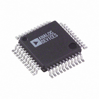
IC ADC 14BIT DUAL 4CHAN 44-MQFP
Manufacturer
Analog Devices Inc
Datasheet
1.AD7864ASZ-1.pdf
(28 pages)
Specifications of AD7864ASZ-2
Data Interface
Parallel
Number Of Bits
12
Sampling Rate (per Second)
520k
Number Of Converters
1
Power Dissipation (max)
120mW
Voltage Supply Source
Analog and Digital
Operating Temperature
-40°C ~ 85°C
Mounting Type
Surface Mount
Package / Case
44-MQFP, 44-PQFP
Resolution (bits)
12bit
Sampling Rate
500kSPS
Input Channel Type
Single Ended
Supply Voltage Range - Analog
4.75V To 5.25V
Supply Current
24mA
Digital Ic Case Style
QFP
Number Of Elements
1
Resolution
12Bit
Architecture
SAR
Sample Rate
520KSPS
Input Polarity
Unipolar
Input Type
Voltage
Rated Input Volt
2.5/5V
Differential Input
No
Power Supply Requirement
Analog and Digital
Single Supply Voltage (typ)
5V
Single Supply Voltage (min)
4.75V
Single Supply Voltage (max)
5.25V
Dual Supply Voltage (typ)
Not RequiredV
Dual Supply Voltage (min)
Not RequiredV
Dual Supply Voltage (max)
Not RequiredV
Power Dissipation
120mW
Differential Linearity Error
±0.9LSB
Integral Nonlinearity Error
±1LSB
Operating Temp Range
-40C to 85C
Operating Temperature Classification
Industrial
Mounting
Surface Mount
Pin Count
44
Package Type
MQFP
Input Signal Type
Single-Ended
Lead Free Status / RoHS Status
Lead free / RoHS Compliant
Lead Free Status / RoHS Status
Lead free / RoHS Compliant, Lead free / RoHS Compliant
Available stocks
Company
Part Number
Manufacturer
Quantity
Price
Company:

Part Number:
AD7864ASZ-2
Manufacturer:
Analog Devices Inc
Quantity:
135
Company:
Part Number:
AD7864ASZ-2
Manufacturer:
Analog Devices Inc
Quantity:
10 000
Part Number:
AD7864ASZ-2
Manufacturer:
ADI/亚德诺
Quantity:
20 000
Company:
Part Number:
AD7864ASZ-2REEL
Manufacturer:
Analog Devices Inc
Quantity:
10 000


PIN CONFIGURATION AND FUNCTION DESCRIPTIONS
Table 4. Pin Function Descriptions
Pin No.
1
2
3
4
5
6
7 to 10
11
12
13 to 16
17
18 to 21
22
23
24
25
26
Mnemonic
BUSY
FRSTDATA
CONVST
CS
RD
WR
SL1 to SL4
H /S SEL
AGND
V
AGND
V
STBY
V
V
AV
AGND
IN4x
IN2x
REF
REF
DD
GND
, V
, V
IN3x
IN1x
Analog Ground. General analog ground. Connect this AGND pin to the AGND plane of the system.
Analog Ground. Analog ground reference for the attenuator circuitry. Connect this AGND pin to the AGND plane
Reference Ground. This is the ground reference for the on-chip reference buffer of the part. Connect the
Analog Ground. Analog ground reference for the DAC circuitry.
Description
Busy Output. The busy output is triggered high by the rising edge of CONVST and remains high until conversion
is completed on all selected channels.
First Data Output. FRSTDATA is a logic output which, when high, indicates that the output data register pointer
is addressing Register 1—see the Accessing the Output Data Registers section.
Convert Start Input. Logic input. A low-to-high transition on this input puts all track-and-holds into their hold
mode and starts conversion on the selected channels. In addition, the state of the channel sequence selection is
also latched on the rising edge of CONVST .
Chip Select Input. Active low logic input. The device is selected when this input is active.
Read Input. Active low logic input that is used in conjunction with CS low to enable the data outputs. Ensure the
WR pin is at logic high while performing a read operation.
Write Input. A rising edge on the WR input, with CS low and RD high, latches the logic state on DB0 to DB3 into
the channel select register.
Hardware Channel Select. Conversion sequence selection can also be made via the SL1 to SL4 pins if H /S SEL is
Logic 0. The selection is latched on the rising edge of CONVST . See the
Hardware/Software Select Input. When this pin is at Logic 0, the AD7864 conversion sequence selection is
controlled via the SL1 to SL4 input pins. When this pin is at Logic 1, the sequence is controlled via the channel
select register. See the Selecting a Conversion Sequence section.
Analog Inputs. See the Analog Input section.
of the system.
Analog Inputs. See the Analog Input section.
Standby Mode Input. TTL-compatible input that is used to put the device into the power save or standby mode.
The STBY input is high for normal operation and low for standby operation.
V
Reference Input/Output. This pin provides access to the internal reference (2.5 V ± 5%) and also allows the
internal reference to be overdriven by an external reference source (2.5 V). Connect a 0.1 μF decoupling
capacitor between this pin and AGND.
Analog Positive Supply Voltage, 5.0 V ± 5%.
REF
GND pin to the AGND plane of the system.
FRSTDAT
CONVST
H/S SEL
BUSY
SL1
SL2
SL3
SL4
WR
RD
CS
A
10
11
1
2
3
4
5
6
7
8
9
44
12 13 14 15 16 17 18 19 20 21 22
43
PIN 1
Figure 3. Pin Configuration
42
Rev. D | Page 7 of 28
41
(Not to Scale)
AD7864
TOP VIEW
40
39
38
37
36
35
34
33
32
31
30
29
28
27
26
25
24
23
DB7
DB8
DB9
DB10
DB11
CLKIN
INT/EXT CLK
AGND
AV
V
V
REF
REF
DD
GND
Selecting a Conversion Sequence
AD7864
section.
Related parts for AD7864ASZ-2
Image
Part Number
Description
Manufacturer
Datasheet
Request
R

Part Number:
Description:
RF/COAXIAL ADAPTER, TRB JACK-TRB JACK
Manufacturer:
TROMPETER ELECTRONICS
Datasheet:

Part Number:
Description:
±1.7g Dual-Axis IMEMS Accelerometer Evaluation Board
Manufacturer:
Analog Devices Inc
Datasheet:

Part Number:
Description:
Inertial Sensor Evaluation System
Manufacturer:
Analog Devices Inc
Datasheet:
Part Number:
Description:
Manufacturer:
Analog Devices Inc
Datasheet:
Part Number:
Description:
Manufacturer:
Analog Devices Inc
Datasheet:
Part Number:
Description:
Manufacturer:
Analog Devices Inc
Datasheet:
Part Number:
Description:
Manufacturer:
Analog Devices Inc
Datasheet:
Part Number:
Description:
Manufacturer:
Analog Devices Inc
Datasheet:
Part Number:
Description:
Manufacturer:
Analog Devices Inc
Datasheet:
Part Number:
Description:
Manufacturer:
Analog Devices Inc
Datasheet:
Part Number:
Description:
Manufacturer:
Analog Devices Inc
Datasheet:
Part Number:
Description:
Manufacturer:
Analog Devices Inc
Datasheet:
Part Number:
Description:
Manufacturer:
Analog Devices Inc
Datasheet: